This thread has been locked.

If you have a related question, please click the "Ask a related question" button in the top right corner. The newly created question will be automatically linked to this question.

SN65HVD1781-Q1: Clarification on RS-485 Bus Configuration

Part Number: SN65HVD1781-Q1
Other Parts Discussed in Thread: ESDS552

Tool/software:

Hi Team,

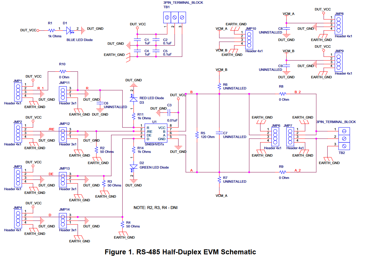
We are currently operating our RS-485 bus at 3.3 V and would like to clarify the following regarding the reserved, unpopulated pull-up and pull-down resistors:

  1. Resistor Values When Unpopulated:

    • What are the recommended resistor values for the unpopulated pull-up (R7) and pull-down (R6) resistors?

  2. Idle Voltage Levels:

    • What are the expected idle voltage levels on lines A and B?

  3. VCM_A and VCM_B Voltage Levels:

    • What should the voltage levels be for VCM_A and VCM_B?

  4. Resistor Values for VCM_A (3.3 V) and VCM_B (GND):

    • If VCM_A is set to 3.3 V and VCM_B is tied to GND, what should the values of R6 and R7 be for a 1.2 km bus length?

  5. Termination Resistor (120 Ω):

    • Under what conditions is the 120 Ω termination resistor required?

Thank you for your support in clarifying these points. Please let me know if you need any additional details.


  • 1. They are not recommended to be populated, except when your system design requires a positive differential voltage on an idle bus.

    2. Without R6 and R7, A and B are expected to be equal.

    3. They are not needed. When you use them, your VCC and GND are the easiest options, but you could use other power rails.

    4. The purpose of the fail-safe resistors is to generate a differential voltage over the two termination resitors. The SN65HVD1781-Q1 requires 0 V, but if you have receivers that require a larger voltage of if you want to increase the noise margin, use resistors that are strong enough. (For 200 mV, you would require resistors with less than 465 Ω.) Please note that the entire bus requires only one set of fail-safe resistors.

    5. A bus should have exactly two termination resistors, at the two ends of the bus.

  • Resistor Values When Unpopulated:

    • What are the recommended resistor values for the unpopulated pull-up (R7) and pull-down (R6) resistors?

    As Clemens pointed out, this is for external fail safe biasing which helps devices without internal fail safe biasing and adds additional noise margin when the bus is ideal. It is not required but can be added for the benefits listed. 

    https://www.ti.com/lit/an/slyt324/slyt324.pdf?ts=1752610361596&ref_url=https%253A%252F%252Fwww.google.com%252F

    Idle Voltage Levels:

    • What are the expected idle voltage levels on lines A and B?

    With R5 populated, Clemens is correct. They will be equal if the driver is disabled. 

    VCM_A and VCM_B Voltage Levels:

    • What should the voltage levels be for VCM_A and VCM_B?

    As Clemens pointed out, they are typically Vcc/GND where A is generally referenced to Vcc and B is generally referenced to GND. 

    Resistor Values for VCM_A (3.3 V) and VCM_B (GND):

    • If VCM_A is set to 3.3 V and VCM_B is tied to GND, what should the values of R6 and R7 be for a 1.2 km bus length?

    See Clemens response but you can refer to this document on external fail safe biasing: https://www.ti.com/lit/an/slyt324/slyt324.pdf?ts=1752610361596&ref_url=https%253A%252F%252Fwww.google.com%252F

    Termination Resistor (120 Ω):

    • Under what conditions is the 120 Ω termination resistor required?

    When the bus is expected to behave like a transmission line. Or another way to put it, if the data rate is faster enough or the distance is long enough that the signal being sent could bounce back and cause signal integrity issues. Terminating the end point with a 120 resistor will dampen the energy that would bounce off the end point in a transmission line.

    Clemens suggestion is correct though, in a half duplex system it is generally recommended that you terminated the two end points.

    -Bobby

  • Dear Bobby,

    In our device, we are using 3.3V field biasing, while the client is using 5V field biasing for the same device. For your reference, please see the attached image.

    Could you kindly confirm if this is acceptable?

    Looking forward to your feedback.

  • Hi Hemal,

    Yes, 3.3V and 5V RS485 transceivers are interoperable. 

    The main thing these transceivers look for is if the VIT+ and VIT- thresholds are met when the A-B voltage is calculated on the receiver side. RS485 drivers are designed around the standard where the voltage should be +/-1.5V w/ a 54 ohm load. Typically speaking, the receiver thresholds for VIT+ max is 200mV and VIT- is -200mV so 1.5V will easily drive both logics.

    -Bobby

  • Dear Bobby,

    We are using 470 Ohm instead of 47T for biasing at 5V RS485 transceivers. Is it create any problem?

  • Sorry Hermal,

    I may have misinterpreted your last post. 

    Are those resistors supposed to be the internal Ron of the PFET and NFETs of the RS485 driver?

    Or are they for external fail safe biasing?

    If so they will be quite strong and the RS485 drivers will have to sink more current when they are actively driving the bus. This can cause VoD to drop. 

    We normally recommend just using one set of external fail safe biasing resistors. If you use two, you need to take the other network into account as the biasing will be much stronger. 

    RS485 limits minimum impedance to be 375 ohms so using a pull up and pull down resistor smaller than 375 would break the standard. 

    Maybe a better question here is what is your intention of having both of the nodes having such strong biasing? 

    -Bobby

  • Hi Bobby,

    Thank you for your detailed explanation and guidance.

    Following up, I’ve attached a snapshot of our RS-485 schematic for your reference. We are using the SN65HVD1781-Q1 transceiver with the following configuration:

    Bus Length: ~1.2 km

    VCC: 3.3V

    Fail-safe Biasing: 560Ω pull-up and pull-down resistors (R249, R250)

    Termination: 120Ω resistor with jumper at one end

    Protection: SM712 and TISP4240M3BJR-S devices

    Based on your input and TI's application notes, we now understand:

    The current fail-safe biasing (560Ω || 560Ω = 280Ω) is stronger than recommended and falls below the 375Ω minimum RS-485 spec.

    Could you kindly confirm the following:

    1) If we change R249 and R250 to 820Ω or 1kΩ, would that be suitable for a 1.2 km bus?

    2) Whether your side already implements fail-safe biasing? If yes, please share the resistor values.

    Looking forward to your confirmation and recommendations.

  • 1) If we change R249 and R250 to 820Ω or 1kΩ, would that be suitable for a 1.2 km bus?

    The external fail safe biasing is really required for all systems. The SN65HVD1781 has internal fail safe biasing (VIT+ is negative) so it technically doesn't require external but having an external fail safe will help if there is differential noise on the bus during open/idle conditions. I personally think you can probably get away with using a 1k resistor. 

    Some other notes with your schematic:

    The RD+/RD- pins could see a negative voltage which would make your protection diodes bias. We generally recommend customer's use bi-directional TVS diodes to support wider common mode ranges. (Over 1.2km cable, the GND between the two nodes will probably not be equal to each other).

    If the device is the receiver node, it's better for the 10 ohm resistors to be placed to the left of the 120 ohm resistor. 

    You can use 3.3V but if you have a 5V rail and intend on driving the signal (instead of receiving) then it's better to use a higher voltage on Vcc to get a larger VoD, this is more important the longer your cable distance is (1.2km is basically the furthest we say RS485 can support).

    -Bobby

  • Dear Bobby,

    Thanks for your detailed feedback on the RS-485 schematic.

    Please find the updated schematic attached for your reference. Let me know if you see anything else that could be improved.

    Thanks again for your support!

  • Hi Hemal,

    the SM712 TVS looks like it would work but I'm not sure about the other diodes (D92/D93). This one looks like it would clamp way too late. 

    You can probably just reuse the SM712 diodes on the individual lines but I can also reassign this thread to the protection devices team and see if they have another recommendation. 

    Also, it looks like the Vcc for the device is 3.3V. Are you doing this because you need to communicate with a 3.3V device? You may be able to use a different RS485 device with a VIO pin and Vcc pin to get better performance. 

    My previous comment about using 5V was on the Vcc of our device though its okay if you use it on the external fail safe.

    Please place a decoupling cap (0.1uF) on Vcc of our device. (The schematic shows it on the GND side which you may need to remember to place next to the device during layout, generally it's placed on the Vcc pin to allow for others to locate it and place on PCB near the pin of interest)

    -Bobby

  • Dear Bobby,

    Thank you for your prompt and insightful feedback on the RS-485 schematic.

    The Vcc is indeed 3.3V to interface with a 3.3V microcontroller.

    Would a 5V pull-up be acceptable for the fail-safe bias configuration in this case?

    I’ve also corrected the decoupling capacitor placement — it is now properly placed on the Vcc pin of the RS-485 device to ensure effective decoupling and easier layout reference.

    Please let me know if you notice anything else that could be improved. Also, feel free to loop in the protection devices team if they might have further recommendations on the TVS selection.

    Thanks again for your continued support.

  • Hi Hemal,

    Would a 5V pull-up be acceptable for the fail-safe bias configuration in this case?

    Yes, that would be fine.

    I'll reassign the thread now to the protection devices team to see if they have any recommendations.

    -Bobby

  • Hi Hemal,

    To protect RS-483 interfaces, TI has ESDS552. It is a 2-channel device in a SOT23 package, so it should be a pin-to-pin replacement for the SM712. ESDS552 also offers higher IEC 61000-4-5 surge rating at 25A, and slightly better clamping voltage. 

    I would definitely replace D92/D93 as those devices don't break down until 200V which is well above the point that components would be taking damage.

    Best,

    Chris