This thread has been locked.

If you have a related question, please click the "Ask a related question" button in the top right corner. The newly created question will be automatically linked to this question.

SN65DSI84: Issue with SN65DSI84 DSI-to-LVDS Bridge Bring-Up on QCS615 Platform

Part Number: SN65DSI84

Tool/software:

Hi Team,


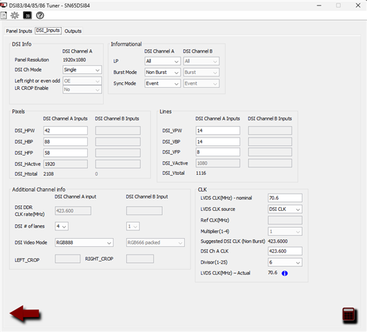
We are currently working on the bring-up of the TI SN65DSI84 DSI-to-LVDS bridge on our QCS615-based platform, running Linux kernel version 6.6.
As part of the validation, we enabled the test pattern generation feature in the SN65DSI84 driver. However, the test pattern displayed on the LVDS panel is unclear and distorted (see attached image for reference).

0181.G133HAN01V1 final spec ver 1.0_20190513.pdf.pdf

static const struct display_timing multi_inno_mi0800ft_9_timing = {
        .pixelclock = { 134000000, 141200000, 149000000 },
        .hactive = { 1920, 1920, 1920 },
        .hfront_porch = { 39, 58, 77 },
        .hback_porch = { 59, 88, 117 },
        .hsync_len = { 28, 42, 56 },
        .vactive = { 1080, 1080, 1080 },
        .vfront_porch = { 3, 8, 11 },
        .vback_porch = { 5, 14, 19 },
        .vsync_len = { 4, 14, 19 },
};

static const struct panel_desc multi_inno_mi0800ft_9 = {
        .timings = &multi_inno_mi0800ft_9_timing,
        .num_timings = 1,
        .bpc = 8,
        .size = {
                .width = 293,
                .height = 165,
        },
        .delay = {
                .prepare = 200,
                .enable = 50,
                .disable = 50,
                .unprepare = 1000,
        },
        .bus_format = MEDIA_BUS_FMT_RGB888_1X7X4_JEIDA,
        .connector_type = DRM_MODE_CONNECTOR_LVDS,
};

// SPDX-License-Identifier: BSD-3-Clause
/*
 * Copyright (c) 2024, Qualcomm Innovation Center, Inc. All rights reserved.
 */
/dts-v1/;

#include "qcs615-smarc.dts"

/ { 
        backlight0: backlight-lcd0 {
    		compatible = "pwm-backlight";
    		//pwms = <&pwm0 0 50000>;  // adjust controller, channel, and period
    		brightness-levels = <0 50 100 150 200 255>;
    		default-brightness-level = <3>;
    		enable-gpios = <&tlmm 115 GPIO_ACTIVE_HIGH>; // LCD0_BKLT_EN
    		pinctrl-names = "default";
    		pinctrl-0 = <&lcd0_bklt_en &lcd0_bklt_pwm>;
	};

	panel-lvds@0 {
                compatible = "multi-inno,mi0800ft-9";
                status = "okay";

                width-mm = <293>;
                height-mm = <165>;
		
//		backlight = <&backlight0>;

                ports {
        	    #address-cells = <1>;
	            #size-cells = <0>;

			port@0 {
				reg = <0>; // LVDS A (Odd pixels)
				dual-lvds-odd-pixels;	
				lvds_panel_out_a: endpoint {
			  	remote-endpoint = <&sn65dsi84_out_a>;
		  		};
			};

			port@1 {
				reg = <1>; // LVDS B (Even pixels)
				dual-lvds-even-pixels;
				lvds_panel_out_b: endpoint {
			 	remote-endpoint = <&sn65dsi84_out_b>;
			  };
			};
                };
        };
};

/delete-node/ &mdss_dsi0_out;

&i2c1 {
        clock-frequency = <400000>;
        status = "okay";

	adv7535@3d {
		status = "disabled";
	};

        sn65dsi84: sn65dsi84@2c {
                compatible = "ti,sn65dsi84";
                reg = <0x2c>;
                enable-gpios = <&tlmm 42 GPIO_ACTIVE_HIGH>;
                ti,dsi-lanes = <4>;
                ti,lvds-format = "jeida-24";
                //ti,lvds-format = <0>;
                ti,lvds-bpp = <24>;
		ti,dual-channel;
		status = "okay";

                ports {
                        #address-cells = <1>;
                        #size-cells = <0>;

                        port@0 {
                                reg = <0>;
                                sn65dsi84_in: endpoint {
                                data-lanes = <0 1 2 3>;
                                remote-endpoint = <&mdss_dsi0_out>;
                                };
                        };

                        port@2 {
                                reg = <2>;
                                sn65dsi84_out_a: endpoint {
                                data-lanes = <0 1 2 3>;
                                remote-endpoint = <&lvds_panel_out_a>;
                                };
                        };
                        
			port@3 {
                                reg = <3>;
                                sn65dsi84_out_b: endpoint {
                                data-lanes = <0 1 2 3>;
                                remote-endpoint = <&lvds_panel_out_b>;
                                };
                        };
                 };
        };
};

&mdss_dsi0 {
    vdda-supply = <&vreg_l11a>;
    status = "okay";

    ports {
        port@1 {
            reg = <1>;
            mdss_dsi0_out: endpoint {
                remote-endpoint = <&sn65dsi84_in>;
                data-lanes = <0 1 2 3>;
                attach-bridge;
            };
        };
    };
};

Additional observations:

When the test pattern is disabled, the LVDS panel only shows the backlight, with no image or signal being displayed.

Our hardware configuration is as follows:
LVDS A carries odd pixels
LVDS B carries even pixels

For your reference, we have attached:

The relevant device tree snippet. (qcs615-smarc-lvds.dts)
The panel settings (panel_timing_settings.txt)
The panel datasheet (G133HAN01V1 final spec ver 1.0_20190513.pdf.pdf)

We would appreciate your guidance in resolving this issue and ensuring proper image display via the SN65DSI84 bridge.

Regards,

Sudarshan

  • Hi Sudarshan,

    Thank you for the background info on the test pattern generation issue. I have a few questions about the setup

    • Is the SN65DSI84 using the DSI CLK or a REF CLK?
    • DSI setup
      • How many DSI lanes used?
      • What is the DSI lane speed/DSI clock frequency?

    If you could attach a I2C register dump of the SN65DSI84, that would be appreciated.

    Best,

    Jack

  • Hi Jack,

    Thanks for the response. Please find my comments below.

    • Is the SN65DSI84 using the DSI CLK or a REF CLK?
      • Sudarshan - SN65DSI84 uses external reference clock of 100MHz (CLK_100MHZ_REFCLK)
    • DSI setup
      • How many DSI lanes used?
      • Sudarshan - 4 lane DSI
      • What is the DSI lane speed/DSI clock frequency?
      • Sudarshan - D-PHY v1.2: 2.1 Gbps/lane on four lanes per port, up to 8.4 Gbps/port
         DisplayPort v1.4 at 5.4 Gbps/lane, 21.6 Gbps/port with support for MST
        Up to a maximum of 5 MP;

    If you could attach a I2C register dump of the SN65DSI84, that would be appreciated.

    Sudarshan - Attached the I2C register dump for reference.

    [   20.003047] sn65dsi83 1-002c: sn65dsi83_probe: Entry
    [   20.003053] sn65dsi83 1-002c: Device matched v[   51.013119] usb usb2-port1: Cannot enable. Maybe the USB cable is bad?
    ia Device Tree
    [   20.003055] sn65dsi83 1-002c: Initializing enable GPIO
    [   20.003086] sn65dsi83 1-002c: Enable GPIO initialized successfully
    [   20.014107] sn65dsi83 1-002c: Parsing device tree
    [   20.014115] Tessolve: sn65dsi83_parse_dt - start
    [   20.014180] sn65dsi83 1-002c: supply vcc not found, using dummy regulator
    [   20.014298] Tessolve: sn65dsi83_parse_dt - end
    [   20.014301] sn65dsi83 1-002c: Initializing I2C regmap
    [   20.014344] sn65dsi83 1-002c: Regmap successfully initialized
    [   20.014346] sn65dsi83 1-002c: Dumping SN65DSI8x registers...
    [   20.014546] sn65dsi83 1-002c: Reg 0x00 = 0x35
    [   20.014724] sn65dsi83 1-002c: Reg 0x01 = 0x38
    [   20.014900] sn65dsi83 1-002c: Reg 0x02 = 0x49
    [   20.015369] sn65dsi83 1-002c: Reg 0x03 = 0x53
    [   20.015572] sn65dsi83 1-002c: Reg 0x04 = 0x44
    [   20.015768] sn65dsi83 1-002c: Reg 0x05 = 0x20
    [   20.015960] sn65dsi83 1-002c: Reg 0x06 = 0x20
    [   20.016156] sn65dsi83 1-002c: Reg 0x07 = 0x20
    [   20.016350] sn65dsi83 1-002c: Reg 0x08 = 0x01
    [   20.016358] sn65dsi83 1-002c: Reg 0x09 = read error
    [   20.016556] sn65dsi83 1-002c: Reg 0x0A = 0x0A
    [   20.016739] sn65dsi83 1-002c: Reg 0x0B = 0x00
    [   20.016742] sn65dsi83 1-002c: Reg 0x0C = read error
    [   20.016918] sn65dsi83 1-002c: Reg 0x0D = 0x00
    [   20.016920] sn65dsi83 1-002c: Reg 0x0E = read error
    [   20.016922] sn65dsi83 1-002c: Reg 0x0F = read error
    [   20.017100] sn65dsi83 1-002c: Reg 0x10 = 0x3E
    [   20.017276] sn65dsi83 1-002c: Reg 0x11 = 0x00
    [   20.017452] sn65dsi83 1-002c: Reg 0x12 = 0x00
    [   20.017454] sn65dsi83 1-002c: Reg 0x13 = read error
    [   20.017456] sn65dsi83 1-002c: Reg 0x14 = read error
    [   20.017458] sn65dsi83 1-002c: Reg 0x15 = read error
    [   20.017460] sn65dsi83 1-002c: Reg 0x16 = read error
    [   20.017461] sn65dsi83 1-002c: Reg 0x17 = read error
    [   20.017637] sn65dsi83 1-002c: Reg 0x18 = 0x70
    [   20.017814] sn65dsi83 1-002c: Reg 0x19 = 0x05
    [   20.017991] sn65dsi83 1-002c: Reg 0x1A = 0x03
    [   20.018167] sn65dsi83 1-002c: Reg 0x1B = 0x00
    [   20.018169] sn65dsi83 1-002c: Reg 0x1C = read error
    [   20.018170] sn65dsi83 1-002c: Reg 0x1D = read error
    [   20.018172] sn65dsi83 1-002c: Reg 0x1E = read error
    [   20.018174] sn65dsi83 1-002c: Reg 0x1F = read error
    [   20.018354] sn65dsi83 1-002c: Reg 0x20 = 0x00
    [   20.018531] sn65dsi83 1-002c: Reg 0x21 = 0x00
    [   20.018532] sn65dsi83 1-002c: Reg 0x22 = read error
    [   20.018534] sn65dsi83 1-002c: Reg 0x23 = read error
    [   20.018710] sn65dsi83 1-002c: Reg 0x24 = 0x00
    [   20.018887] sn65dsi83 1-002c: Reg 0x25 = 0x00
    [   20.018889] sn65dsi83 1-002c: Reg 0x26 = read error
    [   20.018891] sn65dsi83 1-002c: Reg 0x27 = read error
    [   20.019067] sn65dsi83 1-002c: Reg 0x28 = 0x00
    [   20.019244] sn65dsi83 1-002c: Reg 0x29 = 0x00
    [   20.019246] sn65dsi83 1-002c: Reg 0x2A = read error
    [   20.019247] sn65dsi83 1-002c: Reg 0x2B = read error
    [   20.019423] sn65dsi83 1-002c: Reg 0x2C = 0x00
    [   20.019600] sn65dsi83 1-002c: Reg 0x2D = 0x00
    [   20.019602] sn65dsi83 1-002c: Reg 0x2E = read error
    [   20.019605] sn65dsi83 1-002c: Reg 0x2F = read error
    [   20.019781] sn65dsi83 1-002c: Reg 0x30 = 0x00
    [   20.019959] sn65dsi83 1-002c: Reg 0x31 = 0x00
    [   20.019961] sn65dsi83 1-002c: Reg 0x32 = read error
    [   20.019963] sn65dsi83 1-002c: Reg 0x33 = read error
    [   20.020142] sn65dsi83 1-002c: Reg 0x34 = 0x00
    [   20.020146] sn65dsi83 1-002c: Reg 0x35 = read error
    [   20.020322] sn65dsi83 1-002c: Reg 0x36 = 0x00
    [   20.020324] sn65dsi83 1-002c: Reg 0x37 = read error
    [   20.020501] sn65dsi83 1-002c: Reg 0x38 = 0x00
    [   20.020503] sn65dsi83 1-002c: Reg 0x39 = read error
    [   20.020679] sn65dsi83 1-002c: Reg 0x3A = 0x00
    [   20.020683] sn65dsi83 1-002c: Reg 0x3B = read error
    [   20.020864] sn65dsi83 1-002c: Reg 0x3C = 0x00
    [   20.020867] sn65dsi83 1-002c: Reg 0x3D = read error
    [   20.020868] sn65dsi83 1-002c: Reg 0x3E = read error
    [   20.020870] sn65dsi83 1-002c: Reg 0x3F = read error
    [   20.020872] sn65dsi83 1-002c: Reg 0x40 = read error
    [   20.020874] sn65dsi83 1-002c: Reg 0x41 = read error
    [   20.020875] sn65dsi83 1-002c: Reg 0x42 = read error
    [   20.020877] sn65dsi83 1-002c: Reg 0x43 = read error
    [   20.020879] sn65dsi83 1-002c: Reg 0x44 = read error
    [   20.020880] sn65dsi83 1-002c: Reg 0x45 = read error
    [   20.020882] sn65dsi83 1-002c: Reg 0x46 = read error
    [   20.020884] sn65dsi83 1-002c: Reg 0x47 = read error
    [   20.020886] sn65dsi83 1-002c: Reg 0x48 = read error
    [   20.020887] sn65dsi83 1-002c: Reg 0x49 = read error
    [   20.020889] sn65dsi83 1-002c: Reg 0x4A = read error
    [   20.020891] sn65dsi83 1-002c: Reg 0x4B = read error
    [   20.020893] sn65dsi83 1-002c: Reg 0x4C = read error
    [   20.020894] sn65dsi83 1-002c: Reg 0x4D = read error
    [   20.020896] sn65dsi83 1-002c: Reg 0x4E = read error
    [   20.020898] sn65dsi83 1-002c: Reg 0x4F = read error
    [   20.020900] sn65dsi83 1-002c: Reg 0x50 = read error
    [   20.020901] sn65dsi83 1-002c: Reg 0x51 = read error
    [   20.020903] sn65dsi83 1-002c: Reg 0x52 = read error
    [   20.020904] sn65dsi83 1-002c: Reg 0x53 = read error
    [   20.020906] sn65dsi83 1-002c: Reg 0x54 = read error
    [   20.020908] sn65dsi83 1-002c: Reg 0x55 = read error
    [   20.020910] sn65dsi83 1-002c: Reg 0x56 = read error
    [   20.020912] sn65dsi83 1-002c: Reg 0x57 = read error
    [   20.020913] sn65dsi83 1-002c: Reg 0x58 = read error
    [   20.020915] sn65dsi83 1-002c: Reg 0x59 = read error
    [   20.020917] sn65dsi83 1-002c: Reg 0x5A = read error
    [   20.020918] sn65dsi83 1-002c: Reg 0x5B = read error
    [   20.020920] sn65dsi83 1-002c: Reg 0x5C = read error
    [   20.020922] sn65dsi83 1-002c: Reg 0x5D = read error
    [   20.020924] sn65dsi83 1-002c: Reg 0x5E = read error
    [   20.020926] sn65dsi83 1-002c: Reg 0x5F = read error
    [   20.020928] sn65dsi83 1-002c: Reg 0x60 = read error
    [   20.020930] sn65dsi83 1-002c: Reg 0x61 = read error
    [   20.020931] sn65dsi83 1-002c: Reg 0x62 = read error
    [   20.020933] sn65dsi83 1-002c: Reg 0x63 = read error
    [   20.020935] sn65dsi83 1-002c: Reg 0x64 = read error
    [   20.020936] sn65dsi83 1-002c: Reg 0x65 = read error
    [   20.020938] sn65dsi83 1-002c: Reg 0x66 = read error
    [   20.020940] sn65dsi83 1-002c: Reg 0x67 = read error
    [   20.020942] sn65dsi83 1-002c: Reg 0x68 = read error
    [   20.020943] sn65dsi83 1-002c: Reg 0x69 = read error
    [   20.020945] sn65dsi83 1-002c: Reg 0x6A = read error
    [   20.020947] sn65dsi83 1-002c: Reg 0x6B = read error
    [   20.020948] sn65dsi83 1-002c: Reg 0x6C = read error
    [   20.020950] sn65dsi83 1-002c: Reg 0x6D = read error
    [   20.020952] sn65dsi83 1-002c: Reg 0x6E = read error
    [   20.020954] sn65dsi83 1-002c: Reg 0x6F = read error
    [   20.020955] sn65dsi83 1-002c: Reg 0x70 = read error
    [   20.020957] sn65dsi83 1-002c: Reg 0x71 = read error
    [   20.020958] sn65dsi83 1-002c: Reg 0x72 = read error
    [   20.020960] sn65dsi83 1-002c: Reg 0x73 = read error
    [   20.020961] sn65dsi83 1-002c: Reg 0x74 = read error
    [   20.020964] sn65dsi83 1-002c: Reg 0x75 = read error
    [   20.020965] sn65dsi83 1-002c: Reg 0x76 = read error
    [   20.020967] sn65dsi83 1-002c: Reg 0x77 = read error
    [   20.020969] sn65dsi83 1-002c: Reg 0x78 = read error
    [   20.020971] sn65dsi83 1-002c: Reg 0x79 = read error
    [   20.020973] sn65dsi83 1-002c: Reg 0x7A = read error
    [   20.020974] sn65dsi83 1-002c: Reg 0x7B = read error
    [   20.020976] sn65dsi83 1-002c: Reg 0x7C = read error
    [   20.020978] sn65dsi83 1-002c: Reg 0x7D = read error
    [   20.020980] sn65dsi83 1-002c: Reg 0x7E = read error
    [   20.020982] sn65dsi83 1-002c: Reg 0x7F = read error
    [   20.020983] sn65dsi83 1-002c: Reg 0x80 = read error
    [   20.020985] sn65dsi83 1-002c: Reg 0x81 = read error
    [   20.020987] sn65dsi83 1-002c: Reg 0x82 = read error
    [   20.020988] sn65dsi83 1-002c: Reg 0x83 = read error
    [   20.020991] sn65dsi83 1-002c: Reg 0x84 = read error
    [   20.020992] sn65dsi83 1-002c: Reg 0x85 = read error
    [   20.020994] sn65dsi83 1-002c: Reg 0x86 = read error
    [   20.020997] sn65dsi83 1-002c: Reg 0x87 = read error
    [   20.020998] sn65dsi83 1-002c: Reg 0x88 = read error
    [   20.021000] sn65dsi83 1-002c: Reg 0x89 = read error
    [   20.021001] sn65dsi83 1-002c: Reg 0x8A = read error
    [   20.021003] sn65dsi83 1-002c: Reg 0x8B = read error
    [   20.021005] sn65dsi83 1-002c: Reg 0x8C = read error
    [   20.021007] sn65dsi83 1-002c: Reg 0x8D = read error
    [   20.021009] sn65dsi83 1-002c: Reg 0x8E = read error
    [   20.021010] sn65dsi83 1-002c: Reg 0x8F = read error
    [   20.021012] sn65dsi83 1-002c: Reg 0x90 = read error
    [   20.021014] sn65dsi83 1-002c: Reg 0x91 = read error
    [   20.021016] sn65dsi83 1-002c: Reg 0x92 = read error
    [   20.021017] sn65dsi83 1-002c: Reg 0x93 = read error
    [   20.021020] sn65dsi83 1-002c: Reg 0x94 = read error
    [   20.021022] sn65dsi83 1-002c: Reg 0x95 = read error
    [   20.021023] sn65dsi83 1-002c: Reg 0x96 = read error
    [   20.021025] sn65dsi83 1-002c: Reg 0x97 = read error
    [   20.021027] sn65dsi83 1-002c: Reg 0x98 = read error
    [   20.021029] sn65dsi83 1-002c: Reg 0x99 = read error
    [   20.021030] sn65dsi83 1-002c: Reg 0x9A = read error
    [   20.021033] sn65dsi83 1-002c: Reg 0x9B = read error
    [   20.021035] sn65dsi83 1-002c: Reg 0x9C = read error
    [   20.021037] sn65dsi83 1-002c: Reg 0x9D = read error
    [   20.021038] sn65dsi83 1-002c: Reg 0x9E = read error
    [   20.021040] sn65dsi83 1-002c: Reg 0x9F = read error
    [   20.021042] sn65dsi83 1-002c: Reg 0xA0 = read error
    [   20.021043] sn65dsi83 1-002c: Reg 0xA1 = read error
    [   20.021046] sn65dsi83 1-002c: Reg 0xA2 = read error
    [   20.021047] sn65dsi83 1-002c: Reg 0xA3 = read error
    [   20.021049] sn65dsi83 1-002c: Reg 0xA4 = read error
    [   20.021050] sn65dsi83 1-002c: Reg 0xA5 = read error
    [   20.021052] sn65dsi83 1-002c: Reg 0xA6 = read error
    [   20.021054] sn65dsi83 1-002c: Reg 0xA7 = read error
    [   20.021055] sn65dsi83 1-002c: Reg 0xA8 = read error
    [   20.021057] sn65dsi83 1-002c: Reg 0xA9 = read error
    [   20.021058] sn65dsi83 1-002c: Reg 0xAA = read error
    [   20.021060] sn65dsi83 1-002c: Reg 0xAB = read error
    [   20.021061] sn65dsi83 1-002c: Reg 0xAC = read error
    [   20.021063] sn65dsi83 1-002c: Reg 0xAD = read error
    [   20.021064] sn65dsi83 1-002c: Reg 0xAE = read error
    [   20.021066] sn65dsi83 1-002c: Reg 0xAF = read error
    [   20.021068] sn65dsi83 1-002c: Reg 0xB0 = read error
    [   20.021069] sn65dsi83 1-002c: Reg 0xB1 = read error
    [   20.021071] sn65dsi83 1-002c: Reg 0xB2 = read error
    [   20.021073] sn65dsi83 1-002c: Reg 0xB3 = read error
    [   20.021074] sn65dsi83 1-002c: Reg 0xB4 = read error
    [   20.021076] sn65dsi83 1-002c: Reg 0xB5 = read error
    [   20.021077] sn65dsi83 1-002c: Reg 0xB6 = read error
    [   20.021080] sn65dsi83 1-002c: Reg 0xB7 = read error
    [   20.021081] sn65dsi83 1-002c: Reg 0xB8 = read error
    [   20.[   51.981138] usb usb2-port1: Cannot enable. Maybe the USB cable is bad?
    021083] sn65dsi83 1-002c: Reg 0xB9 = read error
    [   20.021085] sn65dsi83 1-002c: Reg 0xBA = read error
    [   20.021087] sn65dsi83 1-002c: Reg 0xBB = read error
    [   20.021088] sn65dsi83 1-002c: Reg 0xBC = read error
    [   20.021090] sn65dsi83 1-002c: Reg 0xBD = read error
    [   20.021092] sn65dsi83 1-002c: Reg 0xBE = read error
    [   20.021094] sn65dsi83 1-002c: Reg 0xBF = read error
    [   20.021095] sn65dsi83 1-002c: Reg 0xC0 = read error
    [   20.021097] sn65dsi83 1-002c: Reg 0xC1 = read error
    [   20.021099] sn65dsi83 1-002c: Reg 0xC2 = read error
    [   20.021100] sn65dsi83 1-002c: Reg 0xC3 = read error
    [   20.021102] sn65dsi83 1-002c: Reg 0xC4 = read error
    [   20.021104] sn65dsi83 1-002c: Reg 0xC5 = read error
    [   20.021105] sn65dsi83 1-002c: Reg 0xC6 = read error
    [   20.021108] sn65dsi83 1-002c: Reg 0xC7 = read error
    [   20.021110] sn65dsi83 1-002c: Reg 0xC8 = read error
    [   20.021111] sn65dsi83 1-002c: Reg 0xC9 = read error
    [   20.021113] sn65dsi83 1-002c: Reg 0xCA = read error
    [   20.021114] sn65dsi83 1-002c: Reg 0xCB = read error
    [   20.021116] sn65dsi83 1-002c: Reg 0xCC = read error
    [   20.021118] sn65dsi83 1-002c: Reg 0xCD = read error
    [   20.021120] sn65dsi83 1-002c: Reg 0xCE = read error
    [   20.021122] sn65dsi83 1-002c: Reg 0xCF = read error
    [   20.021123] sn65dsi83 1-002c: Reg 0xD0 = read error
    [   20.021125] sn65dsi83 1-002c: Reg 0xD1 = read error
    [   20.021127] sn65dsi83 1-002c: Reg 0xD2 = read error
    [   20.021128] sn65dsi83 1-002c: Reg 0xD3 = read error
    [   20.021130] sn65dsi83 1-002c: Reg 0xD4 = read error
    [   20.021131] sn65dsi83 1-002c: Reg 0xD5 = read error
    [   20.021133] sn65dsi83 1-002c: Reg 0xD6 = read error
    [   20.021134] sn65dsi83 1-002c: Reg 0xD7 = read error
    [   20.021136] sn65dsi83 1-002c: Reg 0xD8 = read error
    [   20.021138] sn65dsi83 1-002c: Reg 0xD9 = read error
    [   20.021139] sn65dsi83 1-002c: Reg 0xDA = read error
    [   20.021141] sn65dsi83 1-002c: Reg 0xDB = read error
    [   20.021143] sn65dsi83 1-002c: Reg 0xDC = read error
    [   20.021145] sn65dsi83 1-002c: Reg 0xDD = read error
    [   20.021147] sn65dsi83 1-002c: Reg 0xDE = read error
    [   20.021149] sn65dsi83 1-002c: Reg 0xDF = read error
    [   20.021327] sn65dsi83 1-002c: Reg 0xE0 = 0x00
    [   20.021504] sn65dsi83 1-002c: Reg 0xE1 = 0x00
    [   20.021506] sn65dsi83 1-002c: Reg 0xE2 = read error
    [   20.021507] sn65dsi83 1-002c: Reg 0xE3 = read error
    [   20.021509] sn65dsi83 1-002c: Reg 0xE4 = read error
    [   20.021685] sn65dsi83 1-002c: Reg 0xE5 = 0x01
    [   20.021687] sn65dsi83 1-002c: Reg 0xE6 = read error
    [   20.021688] sn65dsi83 1-002c: Reg 0xE7 = read error
    [   20.021690] sn65dsi83 1-002c: Reg 0xE8 = read error
    [   20.021691] sn65dsi83 1-002c: Reg 0xE9 = read error
    [   20.021693] sn65dsi83 1-002c: Reg 0xEA = read error
    [   20.021695] sn65dsi83 1-002c: Reg 0xEB = read error
    [   20.021696] sn65dsi83 1-002c: Reg 0xEC = read error
    [   20.021698] sn65dsi83 1-002c: Reg 0xED = read error
    [   20.021699] sn65dsi83 1-002c: Reg 0xEE = read error
    [   20.021701] sn65dsi83 1-002c: Reg 0xEF = read error
    [   20.021702] sn65dsi83 1-002c: Reg 0xF0 = read error
    [   20.021704] sn65dsi83 1-002c: Reg 0xF1 = read error
    [   20.021705] sn65dsi83 1-002c: Reg 0xF2 = read error
    [   20.021707] sn65dsi83 1-002c: Reg 0xF3 = read error
    [   20.021708] sn65dsi83 1-002c: Reg 0xF4 = read error
    [   20.021710] sn65dsi83 1-002c: Reg 0xF5 = read error
    [   20.021711] sn65dsi83 1-002c: Reg 0xF6 = read error
    [   20.021713] sn65dsi83 1-002c: Reg 0xF7 = read error
    [   20.021714] sn65dsi83 1-002c: Reg 0xF8 = read error
    [   20.021716] sn65dsi83 1-002c: Reg 0xF9 = read error
    [   20.021717] sn65dsi83 1-002c: Reg 0xFA = read error
    [   20.021719] sn65dsi83 1-002c: Reg 0xFB = read error
    [   20.021720] sn65dsi83 1-002c: Reg 0xFC = read error
    [   20.021722] sn65dsi83 1-002c: Reg 0xFD = read error
    [   20.021723] sn65dsi83 1-002c: Reg 0xFE = read error
    [   20.021725] sn65dsi83 1-002c: Reg 0xFF = read error
    [   20.021726] sn65dsi83 1-002c: Setting up DRM bridge
    [   20.021729] sn65dsi83 1-002c: Attaching to DSI host
    [   20.085287] sn65dsi83 1-002c: Probe successful!
    

    Regards,

    Sudarshan

  • Hi Sudarshan,

    Thank you for providing this information. If the display requires a nominal PCLK of 141.14MHz, then it is not clear why an external reference clock of 100MHz is connected to the SN65DSI84. See below description of external reference clock in datasheet.

    Best,

    Jack

  • Hi Jack,

    Thanks for the response.

    We measured the external reference clock and confirmed that 100MHz we could able to get. 

    Need your guidance further to solve the same. Let me know if you need any information from our side.

    Regards,

    Sudarshan

  • Hi Sudarshan,

    One quick correction on my previous response is that the LVDS clock for this display is nominally 70.57MHz because of dual LVDS ports. The AUO datasheet allows for LVDS clocks of 69.22MHz - 73.9MHz. The 100MHz REFCLK will not be an option for this display.

    The other option is to use the DSI channel A clock as the LVDS clock source. The DSI clock must be continuous for it to function as the LVDS clock source. The above datasheet section I sent previously details the steps needed to program the SN65DSI84 for DSI clock reference.

    Do you know the DSI clock frequency for this system?

    Best,

    Jack

  • Hi Jack,

    Thanks for the prompt reply, I was on leave last week. Sorry for the delay.

    As suggested, We thought of using DSI Channel A clock as the LVDS clock source, Below is the driver used.

    URL: https://github.com/nxp-imx/linux-imx/blob/lf-6.12.y/drivers/gpu/drm/bridge/ti-sn65dsi83.c

    As per my understanding above driver uses external clock by default, In order to select DSI Channel A clock is any specific changes required? Please let me know.

    FYI,

    We isolated external reference clock from hardware side.

    Regards,

    Sudarshan

  • Hi Sudarshan,

    For your configuration, we have the following

    • Nominal PCLK = 141.2MHz
    • LVDS CLK = 70.6MHz
    • DSI DDR CLK = 211.8MHz

    In order to enable the DSI channel A clock the following needs to be done

    • Set DSI_CLK_DIVIDER in Register 0xB[7:3]
      • Set this register to 0x10 to divide by 3
    • Set LVDS_CLK_RANGE and HS_CLK_SRC in Register 0xA 
      • Set this register to 0x0b
    • Set CH_DSI_CLK_RANGE Register 0x12
      • Set this register to 0x2a
    • Set PLL_EN Register 0x0D[0] to enable the internal PLL
      • Set this register to 0x01

    I used the DSI tuner tool to calculate the appropriate register values. You can download the DSI tuner tool in the E2E FAQ below.

    E2E Link

    Best,

    Jack

  • Hi Jack,

    Thanks for the reply.

    We did above settings in our driver source to enable Internal clock, but still observing distorted test pattern.

    Attached the i2cdump for reference:

    No size specified (using byte-data access)
         0  1  2  3  4  5  6  7  8  9  a  b  c  d  e  f    0123456789abcdef
    00: 35 38 49 53 44 20 20 20 01 00 0a 10 00 01 00 00    58ISD   ?.??.?..
    10: 26 00 2a 00 00 00 00 00 0f 05 03 00 00 00 00 00    &.*.....???.....
    20: 80 07 00 00 38 04 00 00 21 00 00 00 20 00 00 00    ??..8?..!... ...
    30: 05 00 00 00 50 00 17 00 30 00 03 00 10 00 00 00    ?...P.?.0.?.?...
    40: 00 00 00 00 00 00 00 00 00 00 00 00 00 00 00 00    ................
    50: 00 00 00 00 00 00 00 00 00 00 00 00 00 00 00 00    ................
    60: 00 00 00 00 00 00 00 00 00 00 00 00 00 00 00 00    ................
    70: 00 00 00 00 00 00 00 00 00 00 00 00 00 00 00 00    ................
    80: 00 00 00 00 00 00 00 00 00 00 00 00 00 00 00 00    ................
    90: 00 00 00 00 00 00 00 00 00 00 00 00 00 00 00 00    ................
    a0: 00 00 00 00 00 00 00 00 00 00 00 00 00 00 00 00    ................
    b0: 00 00 00 00 00 00 00 00 00 00 00 00 00 00 00 00    ................
    c0: 00 00 00 00 00 00 00 00 00 00 00 00 00 00 00 00    ................
    d0: 00 00 00 00 00 00 00 00 00 00 00 00 00 00 00 00    ................
    e0: 00 00 00 00 00 01 00 00 00 00 00 00 00 00 00 00    .....?..........
    f0: 00 00 00 00 40 00 00 80 00 00 00 00 00 00 00 00    ....@..?........
    root@qcs615-smarc:~# 
    

    Regards,

    Sudarshan

  • Hi Sudarshan,

    One correction: Set register 0xA to 0xB to enable the LVDS pixel clock to be sourced from the D-PHY clock.

    Best,

    Jack

  • Hi Jack,

    Thanks for the response,

    Can you please provide the setting for the same? Like, Which bit need to set for both 0xA and 0xB register?

    Regards,

    Sudarshan

  • Hi Sudarshan,

    See below

    • Set DSI_CLK_DIVIDER in Register 0xB[7:3]
      • Set this register to 0x10 to divide by 3
    • Set LVDS_CLK_RANGE and HS_CLK_SRC in Register 0xA 
      • Set this register to 0x0b
        • Set Register 0xA[3:1] = 0x5
        • Set Register 0xA[0] = 0x1
    • Set CH_DSI_CLK_RANGE Register 0x12
      • Set this register to 0x2a
    • Set PLL_EN Register 0x0D[0] to enable the internal PLL
      • Set this register to 0x01

    Best,

    Jack

  • Hi Jack,

    Thanks for the response,

    Can we have a call to discuss further? Let me know your available time today or tomorrow?

    Regards,

    Sudarshan

  • Hi Sudarshan,

    I will be out of office until Monday (Aug 18). We can schedule a call for Monday morning Dallas time at 8am which is 6:30pm IST.

    Are you still having issues with the display? Can you send over the latest register dump from the DSI84?

    Best,

    Jack

  • Hi Jack,

    Thanks for the response,

    Can I schedule a call on Monday at 8:00pm IST? Please let me know if this time works for you or if you would prefer an alternative.

    Can you please share your mail-ID?

    Still we are facing issue with display. Attached the latest register dump from the DSI84.

    root@qcs615-smarc:~# i2cdump -f -y 1 0x2c
    No size specified (using byte-data access)
         0  1  2  3  4  5  6  7  8  9  a  b  c  d  e  f    0123456789abcdef
    00: 35 38 49 53 44 20 20 20 01 00 0b 80 00 01 00 00    58ISD   ?.??.?..
    10: 26 00 2a 00 00 00 00 00 0f 05 03 00 00 00 00 00    &.*.....???.....
    20: 80 07 00 00 38 04 00 00 21 00 00 00 20 00 00 00    ??..8?..!... ...
    30: 05 00 00 00 50 00 17 00 30 00 03 00 10 00 00 00    ?...P.?.0.?.?...
    40: 00 00 00 00 00 00 00 00 00 00 00 00 00 00 00 00    ................
    50: 00 00 00 00 00 00 00 00 00 00 00 00 00 00 00 00    ................
    60: 00 00 00 00 00 00 00 00 00 00 00 00 00 00 00 00    ................
    70: 00 00 00 00 00 00 00 00 00 00 00 00 00 00 00 00    ................
    80: 00 00 00 00 00 00 00 00 00 00 00 00 00 00 00 00    ................
    90: 00 00 00 00 00 00 00 00 00 00 00 00 00 00 00 00    ................
    a0: 00 00 00 00 00 00 00 00 00 00 00 00 00 00 00 00    ................
    b0: 00 00 00 00 00 00 00 00 00 00 00 00 00 00 00 00    ................
    c0: 00 00 00 00 00 00 00 00 00 00 00 00 00 00 00 00    ................
    d0: 00 00 00 00 00 00 00 00 00 00 00 00 00 00 00 00    ................
    e0: 00 00 00 00 00 01 00 00 00 00 00 00 00 00 00 00    .....?..........
    f0: 00 00 00 00 40 00 00 80 00 00 00 00 00 00 00 00    ....@..?........
    root@qcs615-smarc:~# 


    Regards,

    Sudarshan

  • Hi Sudarshan,

    Jack is OoO today and will be back on Monday.

  • Hi Sudarshan,

    I sent an email with an invite for a call. We can discuss next steps there.

    Best,

    Jack

  • Hi Sudarshan,

    Thank you for your time on the call today. For tomorrow's call, there will be a live debug to root cause the PATGEN screen distortion.

    When I looked at the latest register dump I saw that Register 0xE5 = 0x1. This means that the SN65DSI84's PLL is unlocked. When I re-entered everything in to the DSI tuner tool, I realized that there are multiple misconfigurations due to LVDS CLK and Horizontal timing being divided by 2 when using dual LVDS mode.

    Instead of writing down the registers as above, I will send screenshots of the DSI tuner tool and the register output from the tool.

    //=====================================================================
    // Filename   : tessolve_dsi84_setup.txt
    //
    //   (C) Copyright 2013 by Texas Instruments Incorporated.
    //   All rights reserved.
    //
    //=====================================================================
    0x09              0x00
    0x0A              0x05
    0x0B              0x28
    0x0D              0x00
    0x10              0x26
    0x11              0x00
    0x12              0x54
    0x13              0x00
    0x18              0x0f
    0x19              0x00
    0x1A              0x03
    0x1B              0x00
    0x20              0xc0
    0x21              0x03
    0x22              0x00
    0x23              0x00
    0x24              0x38
    0x25              0x04
    0x26              0x00
    0x27              0x00
    0x28              0x30
    0x29              0x00
    0x2A              0x00
    0x2B              0x00
    0x2C              0x15
    0x2D              0x00
    0x2E              0x00
    0x2F              0x00
    0x30              0x0e
    0x31              0x00
    0x32              0x00
    0x33              0x00
    0x34              0x1d
    0x35              0x00
    0x36              0x0e
    0x37              0x00
    0x38              0x2c
    0x39              0x00
    0x3A              0x08
    0x3B              0x00
    0x3C              0x10
    0x3D              0x00
    0x3E              0x00
    
    
    The PLL_EN bit and SOFT_RESET bit are not set as they need to be set per the recommended sequence defined in the datasheet

    /resized-image/__size/640x480/__key/communityserver-discussions-components-files/138/first_5F00_page.png

    /resized-image/__size/640x480/__key/communityserver-discussions-components-files/138/second_5F00_page.png

    Best,

    Jack

  • Hi Sudarshan,

    After a couple of meetings to debug the SN65DSI84-Q1, both PATGEN and end-to-end video was successfully brought up. All issues were caused by driver misconfiguration.

    1. PATGEN on SN65DSI84-Q1

    • The root cause of the PATGEN not working as expected was because the driver was incorrectly programming the horizontal video timings in the CSR registers. 
    • When in dual LVDS mode, ALL horizontal timings including horizontal active must be divided by 2. This is the per port LVDS timing

    2. End-to-end video on SN65DSI84-Q1

    • From inspecting the driver and DSI CLK measurement, I had a suspicion that the line timing was not matched between DSI input and LVDS output
    • My suggestion to not use burst timing in the DSI mode flags fixed the issue with end-to-end video.

    Previous Driver Configuration

    Current Driver Configuration

    Best,

    Jack