This thread has been locked.

If you have a related question, please click the "Ask a related question" button in the top right corner. The newly created question will be automatically linked to this question.

THVD1450: TVS diode ground connection

Part Number: THVD1450

Tool/software:

Hi,

I am facing some strange issue.

i am attaching some block diagram of my circuit.


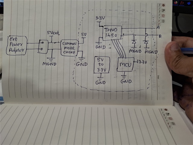
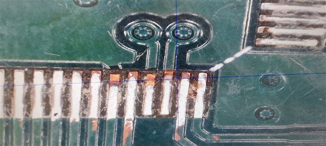
on field, in some PCBs, RX,TX logic lines trace near MCU (pic32) is cut or open or may be burnt ( i am not sure whether it is burnt or not). but it is open for sure. The location is same . it is at mcu pin side always.

but there is no any kind of damage to THVD1450, MCU, TVS diode. even Rx,TX is also working well from MCU. there is no any component damage.

I have applied MGND rather then GND to TVS diode so that surge can pass out from PCB quickly. I have do this because there is common mode choke in return path. so, it may resist the surge.

I am not able to find the cause who has damaged these traces. I have communicated this scenario to Open AI (chatGPT). kindly find below the link for whole communication study.

https://chatgpt.com/share/6877ad4f-94ec-8004-841c-85f4c996fe58

it has explained me that i did the wrong to give MGND to TVS diode & it is the main cause for the trace damage. It also explained me the whole logic behind it. but i am not satisfied with its explanation.

I mean how surge current flow to opposite direction from MGND to GND back (& then to pins,or trace to ICs pin), instead of going to MGND to external adptor directly. Did i make mistake to give MGND to TVS diode instead of GND? 

Regards,

jigar


  • Hi Jigar,

    There should be some kind of connection between MGND and GND to ensure that they see the same GND reference. Otherwise the surge could try to go to GND instead of MGND if the GND was a lower reference than MGND. I sometimes see people do this with a large 1M ohm resistor from chassis GND and digital GND and a cap in parallel. 

    That being said, I'm not sure this is the root cause of the issue. 

    Some of the keepout on the picture seems oxidated or damaged (I don't know if those are actual burn marks) and it seems like its too uniform (the square area is black and in a straight line). I'm wondering if it may be related to the PCB fab shop since the damaged keep out is so straight. 

    I spoke with my colleague who is more experienced in PCB fab than I am and he provided these comments:

    "The amount of exposed copper on the solder pads does seem like a cheap PCB fab process because I would expect some sort of plating such as nickel, tin, lead, gold, etc. that would help with the solder adhesion. Soldering directly to copper isn't the best, or easiest thing to do."

    "The re-work technician seemed like they were not gentle with the board and there is a lot of worn away solder mask spots over the traces from some sort of rubbing or cleaning during the re-work of the board.  This may or may not have attributed to the open trace."

    "one thought I had was that since MGND and GND are connected through the CMC, there may be some sort of kickback voltage or voltage to GND issues when a large current is trying to flow through MGND bypassing the CMC which is trying to maintain equal amounts of current flowing through the 5V supply and GND paths through the CMC. This may be creating enough of an issue to affect some traces. But placing some decoupling capacitors between MGND and GND may help decouple and stabilize the voltage between MGND and GND during a surge event or if the TVS diode"

    -Bobby

  • Hi Bobby,

    Thanks for your replay.

    I am attaching OK PCB trace pic. 

    These PCBs are assembled through Pick & Place Machine. There is no any kind of rework done after PCB assembled.

    When we have faced open trace issue (we have checked using multi meter), then to check from where trace is opened, we have removed MCU using hot air gun.then we have taken the pic & sent you.(you can check in damaged PCB pic)

    same things done in OK PCB & we have given its pic that you can see above.

    in blank PCBs, we have checked that there is no any open copper layer exposed.

    i am attaching a pic which describe my idea behind applying MGND to TVS diode.

    please find here.

    When surge occurs, it will flow from TVS diode -> MGND -> external power adptor. normal current will continue to flow from CMC.

    So, Surge will have the shortest path to move out from PCB via MGND with lowest resistance path.

    And yes, we have chassis ground also which is connected to MGND with parallel combination of 1M resistor & 10nF/2KV capacitor.here we are not facing any issue.

    Is it ok to give MGND to TVS diode?

    Is this happen due to mishandling of blank pcb at assembly production?

    all things are working (TVS diode, THVD1450, MCU, all GPIOs between THVD1450 & MCU) well. only logic lines trace is opened specially those two lines which are passing under MCU via vias. There maybe less amount of chance of surge. please correct me if i am wrong.


    Regards,

    Jigar

  • Hi Jigar,

    And yes, we have chassis ground also which is connected to MGND with parallel combination of 1M resistor & 10nF/2KV capacitor.here we are not facing any issue.

    Is it ok to give MGND to TVS diode?

    This should be a good enough connection to allow for a good reference between both GND planes across frequencies. Since both GND planes are referenced to each other it should be fine to have TVS diode reference MGND since that should be the larger plane and has less chance of disrupting the digital signals. 

    Is this happen due to mishandling of blank pcb at assembly production?

    all things are working (TVS diode, THVD1450, MCU, all GPIOs between THVD1450 & MCU) well. only logic lines trace is opened specially those two lines which are passing under MCU via vias. There maybe less amount of chance of surge. please correct me if i am wrong


    o

    I still think this may be related to the manufacturing of the PCB. I'm wondering if maybe you can make the trace thicker to prevent the trace from breaking. 

    During your testing is the board getting hot and cooling off repeatedly?

    Does MGND sit directly below the trace that is breaking? (Maybe the surge current is heating up the plane beneath it and expanding causing the trace to weaken)

    -Bobby

  • Hi Bobby,

    Thanks for your help.

    I have no further questions.