This thread has been locked.

If you have a related question, please click the "Ask a related question" button in the top right corner. The newly created question will be automatically linked to this question.

TCA39306: VREF1 = 3.3V & VREF2 range is 1.2V to 5V

Part Number: TCA39306
Other Parts Discussed in Thread: USB2ANY, , LSF0102

Tool/software:

Hi TI Expert,

We are currently developing a development tool, a product similar to USB2ANY. The aim is to provide a solution capable of delivering a wide range of I2C voltages (1.2V to 5V) to a remote DUT (Device Under Test), while maintaining specific MCU-side I/O voltages for two I2C channels:

  1. First I2C Channel:

    • Operating in Fast Mode+ (up to 1 MHz).
    • MCU-side I/O voltage: 3.3V.
  2. Second I2C Channel:

    • Operating in High-Speed Mode (3.4 MHz).
    • MCU-side I/O voltage: 1.8V.

We are looking for a voltage level translator that can fulfill these requirements. Ideally, both I2C channel voltage level translators should support a wide range of voltages (1.2V to 5V) at the targeted operating frequencies for the remote DUT.

If it is not possible for both voltage level translators to support the full 1.2V to 5V range, we are open to alternative solutions that meet the operating frequency and voltage requirements for each channel.

1st case we like to evaluate as below: 

  1. First I2C Channel:

    • Operating in Fast Mode+ (up to 1 MHz).
    • MCU-side I/O voltage: 3.3V.
    • Remote DUT side voltage has to support from 1.2V to 3.3V as shown below image. 

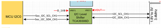
2nd case we like to evaluate as below: 

  1. Second I2C Channel:

    • Operating in High-Speed Mode (3.4 MHz).
    • MCU-side I/O voltage: 1.8V.
    • Remote DUT side voltage has to support from 1.8V to 5V as shown below image. 

We are ok to enable and disable the pull-up resistor using below configuration:

 we have some specific concerns regarding the voltage level translator for our I2C channels. We are seeking your guidance and recommendations to address the following: 

  1. Propagation Delay in HS-Mode:
    When VREF1 equals VREF2, can the I2C voltage translator operate in HS-mode (3.4 Mbit/s) without concerns regarding propagation delay? If not, could you suggest an alternative solution that ensures reliable operation at this speed?

  2. VREF1 > VREF2 Scenario:
    In our application, it is certain that VREF1 voltage will exceed VREF2 (VDUT varies between 1.2V and 5V). Are there any concerns or limitations in this scenario? If yes, what alternative solutions or configurations would you recommend?

  3. Enable Pin Biasing:
    The EN pin must always be biased such that it does not exceed  VREF_1 + Vth = VREF_1+ 0.6 V. However, in our use case, VDUT is expected to vary between 1.2V and 5V, and we are unsure how to drive the Enable pin appropriately. Could you provide guidance or suggest alternative solutions for this requirement?

We would greatly appreciate your input on suitable components, configurations, or design considerations to address these concerns.

Looking forward to your response

Best regards,
Vaibhav Kundariya

  • The two VREF voltages are independent from the pull-up voltages; the only requirement is that VREF1 must not be lower than any pull-up voltage, and that VREF2 must be higher than VREF1.

    So you can use VREF1 = 1.2 V, VREF2 = 3.3 V.

  • Thanks for your feedback. 

    I have one question: Do we not need to connect a pull-up resistor on the VREF2 side of the I2C signal? we need pull up on both side of TCA39306 , correct?  If a pull-up resistor is required on the VREF2 side, then how would the following condition hold true?

    only requirement is that VREF1 must not be lower than any pull-up voltage

    Looking forward to your clarification.

    Best regards,
    Vaibhav Kundariya

  • Hi Vaibhav, 

    Do you have a quick block diagram for reference? 

    Regards,

    Tyler

  • A pull-up resistor is required for any output signal that goes higher than VREF1. So you need pull-ups on both sides.

  • We are currently developing a development tool, a product similar to USB2ANY. The aim is to provide a solution capable of delivering a wide range of I2C voltage (1.2V to 5V) to a remote DUT (Device Under Test), while maintaining an MCU-side voltage of 3.3V for one I2C channel and 1.8V for second I2C channel. 

    The voltage supply to VREF2 or VREF1 will be sourced from the DUT itself, ensuring that the DUT and the level translator output voltage remain consistent.

    We will have max 2 X I2C channel. 

    I have encountered the following design constraint "To support translation, VREF1 supports 0.85 V to VREF2 - 0.6 V. VREF2 must be between VREF1 + 0.6 V to 5.5 V. See Typical Application for more information"

     I am concerned about how to convert the translator mode into switch mode (e.g., 1.8V MCU-side to 1.8V DUT-side) within the same hardware design. We are open to incorporating a logic circuit controlled by firmware to enable switching between translator mode and switch mode.

    Could you please assist in identifying or designing a suitable solution for this requirement?

  • Vaibhav,

    "To support translation, VREF1 supports 0.85 V to VREF2 - 0.6 V. VREF2 must be between VREF1 + 0.6 V to 5.5 V. See Typical Application for more information"

    This is a recommendation to keep level translation fast. It is true if you have 1.8V on VREF2 and 1.8V on VREF1, it technically violates this condition since VREF1 = 0.85V to (1.8V - 0.6V) = 1.2v. 

    If you use TCA39306 in level translation mode, and have VREF1 = VREF2, the device should still work properly for I2C, you might see reduced performance specifically in prop delay - delays will be longer (nanosecond range). This shouldn't affect I2C signals, even at fast mode+ speeds (up to 1 MHz). 

    The key for getting TCA39306 to work properly is to ensure the EN voltage is controlled. 

    TCA39306 internal structure closely follows that of the LSF0102: 

    EN must always be biased so that it never reaches above VREF_A + Vth = VREF_A + 0.6 V. 

    For the first case: 

    VREF1 = VREF2 = 1.8V will be okay even in the voltage translation mode. The device will still function properly, but the prop delays may be slightly slower than characterized. 

    Case 2: 

    VREF2 = VREF1 = 3.3V would be worse case, but would still work even in level translation mode because the EN voltage is still biased to 3.3V. 

    When VREF2=3.3V and VREF1 = 1.2V, the voltage translation connection scheme where VREF2 is shorted to EN, will automatically set the EN voltage = 1.2V + VTH = ~1.8V due to the passFET connecting VREF_A to VREF_B. 

    Regards,

    Tyler

  • Hello TI extert

    Can you please answer to below question:

    If you use TCA39306 in level translation mode, and have VREF1 = VREF2, the device should still work properly for I2C, you might see reduced performance specifically in prop delay - delays will be longer (nanosecond range). This shouldn't affect I2C signals, even at fast mode+ speeds (up to 1 MHz). 

    You have confidence at 1 MHz speed, but for the use case provided above, will I2C work in HS-mode (3.4 Mbit/s) without any concerns regarding propagation delay? What is your opinion on this?

    EN must always be biased so that it never reaches above VREF_A + Vth = VREF_A + 0.6 V. 

    We don't know how to drive the Enable pin in our use case; the VDUT is going to vary between 1.2V and 5V. Do you have any guidance?

    Your guidance is highly valuable in providing the solution.

    -

    Thanks 

  •    &  

    I have updated original query for better clarity.

  • Hi Vaibhav,

    TCA39306 is rated for up to 12.5 MHz I3C speeds. 

    In the switching mode, the VREF1 and VREF2 pins do not need to be connected. The EN pin voltage should not dip below 1.5V. 

    Based off recommended operating conditions, if EN>=1.5V, we can hit the 12.5 MHz target for the device. 3.4 Mbit/s would be well underneath this data rate. 

    We don't know how to drive the Enable pin in our use case; the VDUT is going to vary between 1.2V and 5V. Do you have any guidance?

    Your guidance is highly valuable in providing the solution.

    For case 1: 

    If the TCA39306 is put into level translation mode, even when VREF1 = 3.3V, the device will still work. The passFET connecting VREF1 to VREF2 will be disabled. EN voltage will be pulled up to 3.3V by the 200k resistor. 

    When VREF1 = 1.2V, the voltage translation mode connection will automatically set the EN voltage to the correct voltage for passing signals with good prop delay performance. 

    For case 2: 

    VREF1 = 1.8V, worst case is when VREF2 = 1.8V. The same occurs as in case 1. The passFET connecting VREF1 to VREF2 will be disabled, and a 200k resistor will pull up the EN voltage to 1.8V. 

    When VREF2 = 5V, and the TCA39306 is set in voltage translation configuration, the device will automatically adjust EN voltage to the correct level. 

    This design is valid. 

    Regards,

    Tyler