DS250DF230EVM: SigCon Architect GUI software

Part Number: DS250DF230EVM
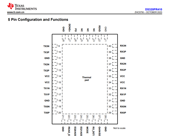
Other Parts Discussed in Thread: DS250DF230, DS320PR410

Tool/software:

Hi,

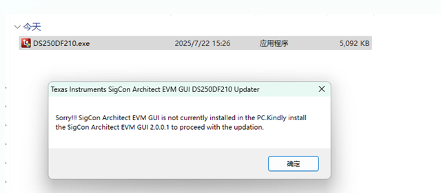
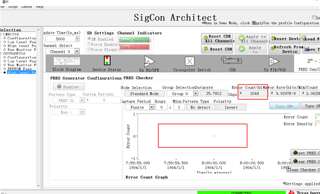
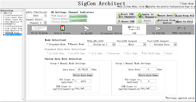
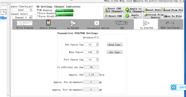
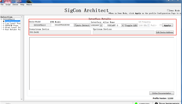
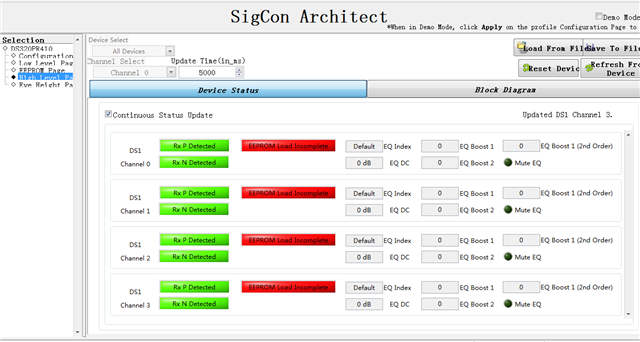
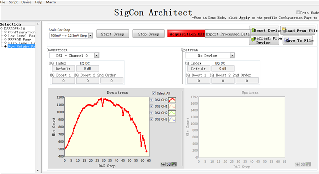
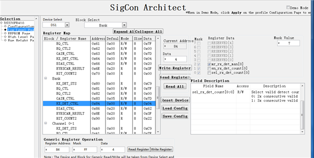
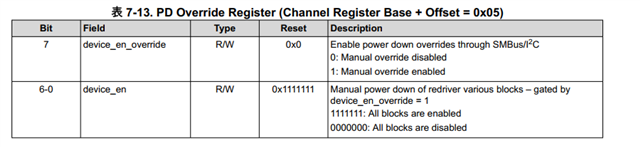
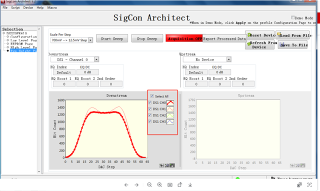
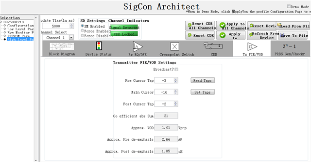
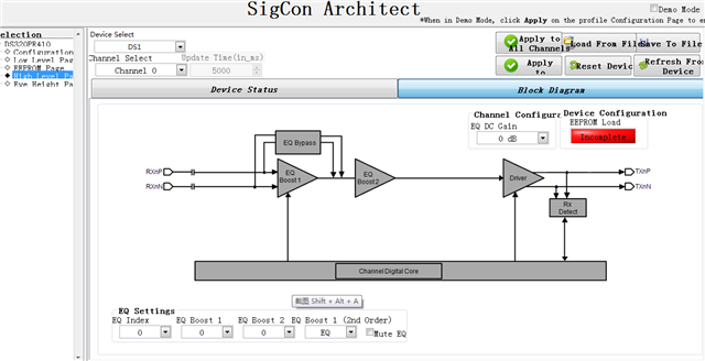
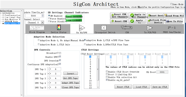
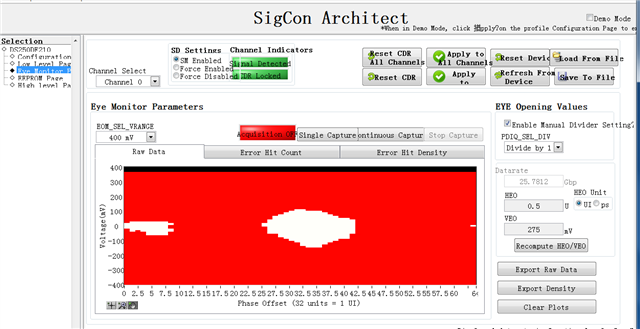
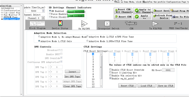
I want to use DS250DF230EVM, after download DS250DF230 device profile and install this program, it has information as below picture.

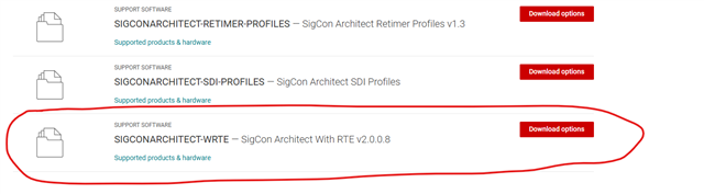
this device profile requeset SigCon Architecture EVM GUI 2.0.0.1, but the oldest software is 2.0.0.8 found in the TI Website, how can I use this software?

Many thanks. 

  • Hi,

    Could you please try installing SigCon Architect with run-time engine (wRTE), and then opening the device profile? 

    Best regards,

    Greg

  • Hi Greg,

    we use this software and give 25.78125Gpbs PRBS31 signal to DS250DF230EVM,  at CDR page we only can Signal detected, but CDR is not locked.

    so could you please give some suggestions about how to debug this problem.

    Many thanks.

  • Hi Greg,

    According to DS250DF230EVM User’s Guide 2.2.4.7 PBRS Tab,  we follow steps listed in 2.2.4.7, it should like  Figure 19 shows in User Guide.

    But we get result as attached,  so would please give some suggestions to debug problems?

    Many thanks.


  • Hi Jianxiang,

    To help with debugging, could you pleasure share a schematic of your setup and/or any non-default register programming implemented in the application?

    Best regards,

    Greg

  • Hi Greg,

    Our application like below picture shows, the setting of chip follows DS2x0DFxx0_Programmers Guider section 5.3 Front-Port Ingress(Table 5-4 25.78125Gbps  Front-Port Ingress Application Configuratin Seq.

    Any more informaion please let me know, many thanks.

  • Hi Jianxiang,

    The DS250DF230 device supports two cal_clk frequencies - 25 MHz and 30.72 MHz. The configuration of the device depends on the frequency being used, which could potentially cause the CDR lock issue. What is the cal_clk frequency used in your setup? 

    Best regards,

    Greg

  • Hi Greg,

    Many thanks,

    we configure REG 0X2F with the value 0X50,  but  I am not sure what does RECOVERED CLOCK FREQUENCY mean in the last column.

  • Hi Jianxiang,

    For the calibration clock,  there should be an external oscillator inputting a 30.72 MHz or 25 MHz single-ended clock to the CAL_CLK_IN pin. Can you check what your input there is? Table 7-7 shows the configuration of the recovered clock frequency for different input data rates. The register 0x2F values stated in the table configure the frequency of the clock recovered from the data stream to the figures shown in the RECOVERED CLOCK FREQUENCY column.

    However, the values in this table are only accurate for a calibration clock set to 30.72 MHz, as indicated in the footnote. 

    Best regards,

    Greg

  • Hi Greg,

    I think we correct errors and make it in the right way.

    As eye diagram shows the signal from Channel 0, is it ok as input signal for DS250DF230 by your experience?

    Many thanks...


  • Hi Greg,

    After we can check quality of input signal, is there any easy way to check quality of DS250DF230 output(especially after a long trace)?

    The frequency of signal is 25.78125G,  if we want to check with oscilloscope then bandwidth will more than 60G hz, it's not easy to find suitable instrument with this spec., so normally how this kind of signal is checked?

    Millions thanks for your kindly support~


  • Hi Jianxiang,

    1. I think the eye diagram looks good. We advise to also look at the HEO/VEO of the eye reported on the device status page - these values are directly from registers 0x27 and 0x28.  We recommend to target HEO and VEO of at least 0.4UI and 200mV, respectively.

    2. The quality of the DS250DF230 output signal can be assessed by evaluating the eye diagram using an oscilloscope. If you do not have an oscilloscope with a high enough bandwidth, a Bit Error Rate Tester can also be used to determine the quality of the output signal. If this device is also not available, the signal can be looped back to the DS250DF230 to roughly measure bit error rate. However, this will be less accurate as the retimer will also adapt to the input signal and apply some CTLE/DFE.

    If you are trying to optimize TX FIR, this article may be helpful. 

    Best regards,

    Greg

  • Hi Greg,

    The HEO is 0.4375UI and VEO is 168.75mV, it seems a bit lower than expected value, we will try to optimize it.

    In current application there is  DS320PR410 connect with the output of this chip,  two channels differential signal of this chip connect to DS320PR410's input.

    we will try to check the function of DS320PR410, if we have some questions we will ask your kindly support.

    Many thanks.

  • Hi Greg,

     We use SigCon software to check function of DS320PR410, two channels inputs come from DS250DF230 TX0/TX1,

     DS250DF230 TX0  =>DS320PR410 RX0

    DS250DF230  TX1 =>DS320PR410 RX1

    DS320PR410 RX2/RX3 channels Left open

    From Eye Height page, DS320PR410 RX0 channel has input but it's not correct, RX1 channel has no input, Is my understanding correct?

    May it be caused by hardware connection or setting of DS320PR410?

    Thanks.

  • Hi Jianxiang,

    Thank you for sharing the screenshots. The figure shown for Channel 0 in the eye height page is not necessarily an incorrect input. More information about the Eye Height Page can be found in the SNLA435A Application Note for PCIe redrivers. For the upstream plot on the right, did you select Channel 1 in the device section? It looks like no device is selected. 

    Also, could you please share further details about your setup? For example, how long are the cables between the DS250DF230 and DS320PR410?

    Best regards,

    Greg

  • Hi Greg,

    Thanks.

    I have snap-shot from PCB file, these two chips are on the same pcb and length of traces is around 4cm.

    so perhaps  I need to verify  signal TX0/TX1 of DS250DF230  correct or not physically, then can make a decsion if therre any problem with  DS320PR410  or not.

    As we input DS250DF230  with 25.78125G PBRS31 signals, after processing of DS250DF230 then Eye Height diagram of DS320PR410 should be like the second picture(If signal is good enough at RX0/RX1 pins of DS320PR410).

    Please correct me is there some mis-understanding in my mind.

    Thanks... 

  • Hi Jianxiang,

    You are correct, the TX0/1 signal of the DS250DF230 should be verified and the eye diagram should resemble the second picture. Apologies for any confusion. For the DS320PR410, what settings are configured for the receiver detect state machine? As you are not sending a PCIe signal here, PD should be low and RX_DET should be L0 to disable PCIe Rx detection state machine. You can reference the settings in the top section of Table 7-3 on the device data sheet.

    Best regards,

    Greg

  • Hi Greg,

    Thank you.

    This project is not a PCIe application and we communicate with DS250DF230 via I2C bus,  so PIN RX_DET/SCL is used as SCL signal, pin PD connect to GND physically.

    Please refer configuration for RX_DET_CTRL as below snap-shot, is this configuration correct?

    By the way, we use SigCon  Architect to configure chip, there is  PD Override Register(table 7-13), but this register is not listed in SigCon Architect program, do we need to configure this register with other tools?
     

    Many thanks...

  • Hi Jianxiang,

    Your RX_DET_CTRL configuration looks correct. The device_en_override register is not included in SigCon Architect, and it is generally not recommended to alter the register. As the default values lead to normal operation of the device, is there a specific reason that your system needs to change the register values?

    Best regards,

    Greg

  • Hi Greg,

    It's ok that device_en_override register default value works.

    Today I take some snap-shots from  output of DS250DF230(ch0/ch1,pic2/pic3 below) and DS320PR410, but Eye-Height diagram of DS320PR410 seems not good(the last pic below).

    We try to modify value DEF/CTLE/FIR and also EQ,but we can see some changes in wave-form/eye-diagram but the change is not obvious.

    Could you please give some suggestions about how to fine-tune parameters and improve signal quality at the output of DS320RP410?

  • Hi Jianxiang,

    Thank you for the additional screenshots. I will take a look and give some potential suggestions for your setup tomorrow.

    Best regards,

    Greg

  • Hi Jianxiang,

    For your design implementation, why is the DS320PR410 connected to the DS250DF230 in the system? Based off of the eye values in these images, the input to he DS250DF230 is not that good. Potentially setting adapt mode 2 could help here. Also, to improve signal quality at the output of the DS320PR410, the TX FIR and VOD can be adjusted on the DS250DF230. For this application CTLE 0 should be set on the DS320PR410. Adjusting gain here may have some trade-offs between eye height and eye width.

    Best regards,

    Greg

  • Hi Greg,

    I'm  coming back again~

    In past days we did some experiments, we input 12.5G/25G PBRS31 signal to DS250DF230 on the board mentioned above , and got eye diagrams at the output of DS320PR410.

    It's obviously that eye diagram at 25Gbps  is not good, is it possible to give some advice to fine-tune parameters of these two chips,or some detailed debug guide? 

    The problem maybe caused by hardware or some setting,we need to find root cause and fix it.Thinking


    The setting of two chips listed as below pictures.


    Many thanks for your kindly support~

  • Hi Jianxiang,

    I have a few further questions. Does the eye diagram measured on the DS320PR410 still look similar to what you previously sent, or did it improve since last time? In addition, what is the length of the cable between the DS320PR410 TX and the oscilloscope used to collect the diagram in your latest update. If you set the Adaptive Mode to Mode 2 on the Rx EQ/DFE page, does the eye diagram improve for 25Gbps?

    Best regards,

    Greg

  • Hi Greg,

    Thank you.

      There is no obvious change in eye diagram at the output of DS320PR410 when we change adaptive mode from mode 0(CTLE only) to mode 2(CTLE w/DFE fine-tune),the cable we used is Huber+Suhner  SUCOFELX 101P RF cable(around 0.5m), but we can see the in VEO which change from 200mv to 275mv(pls. refer below pictures)

    1. snap-shot for MODE 2

    2. snap-shot for MODE 0


    Is there any way to find cause?

    Many thanks.

  • Hi Jianxiang,

    An HEO of 0.5 UI and VEO of 275 mV is a good eye opening, so it seems there is loss after the DS250DF230. Could you please share the HEO and VEO measured on the DS320PR410? Also, if you use a shorter cable between the DS320PR410 and the oscilloscope, do you see an improvement in the eye diagram on the oscilloscope?

    To verify potential loss between devices, what is the PCB material you use in your design?

    Best regards,

    Greg