This thread has been locked.

If you have a related question, please click the "Ask a related question" button in the top right corner. The newly created question will be automatically linked to this question.

TCAN1043-Q1: VIO and VCC, VSUP internal circuit association

Part Number: TCAN1043-Q1

Tool/software:

Dear Experts,

My customer is testing the voltage tolerance of VCC and VSUP and has found the following situations:
When a voltage of 13V is applied to VCC alone, it will cause damage to the VCC and VIO pins, resulting in VCC impedance to ground changing from ∞ to 20M Ω and VIO impedance to ground changing from ∞ to below 100 Ω
When a voltage of 70V is applied to VSUP alone, the impedance of VCC to ground changes from ∞ to 20M Ω, and the impedance of VIO pin to ground changes from ∞ to below 100 Ω

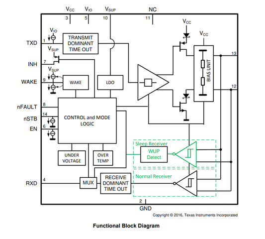
At present, we have seen the internal block diagram of TCAN1043-Q1 in the data manual, where the three pins are not connected together. We would like to know what the internal connections between these three pins are?  Whether it is due to design reasons that may damage VIO when high voltage is applied. Thank you

  • Hi Colin,

    Thanks for reaching out. I am reviewing this and I will get a response to you by EOD tomorrow. 

    Best,

    Ethan

  • Hi Colin,

    Unfortunately, there is nothing really that helpful I can share with you. Because the voltages applied to VCC and VSUP (on the non-H version at least) are above the absolute maximum rating in the datasheet, there is no predictable behavior we can give. 13V on VCC or 70 on VSUP (on the 58V rated version) should be avoided at all costs, and any we do not guarantee any anything else after this damage takes place.

    As for the functional block diagram, it is a general diagram for illustrative purposes as the full block diagram is much more complex and cannot be shared publicly.

    Best,

    Ethan

  • 我们在实际应用中有一个案例,因为VCC引脚有很大的电压注入,导致洗牌损坏,大约10V电压。当我在仿真中重现时,向芯片的VCC引脚注入13V会导致芯片断裂,但是有没有其他方法可以以与实际情况不同的方式再现损坏情况?

    以下是异常芯片的例外情况:
    损坏芯片的阻抗从∞变为40Ω,5pin(VIO)的阻抗从∞变为2MΩ

    谢谢!

  • We have a case in the actual application because the VCC pin has a large voltage injection that causes shuffle damage, about 10V voltage. When I reproduce in the simulation, injecting 13V into the VCC pin of the chip causes the chip to break, but is there any other way to reproduce the damage situation differently than what actually happened?

    Here are the exceptions to the abnormal chip:
    The impedance of the damaged chip changed from ∞ to 40Ω, and the impedance of 5pin (VIO) changed from ∞ to 2MΩ

    Thank you!

  • Hi Jingyang,

    No tests should be performed above 7V on VCC (this is the absolute maximum). 5.5V is the recommended maximum. Voltages above this will likely cause permanent damage, and we cannot provide further support when absolute maximum conditions are violated. If you continually expect +10V to be applied to the VCC pin in your actual application, please add external protection such that it clamps to 7V or lower. A series resistor could also work. 

    Best,

    Ethan