This thread has been locked.

If you have a related question, please click the "Ask a related question" button in the top right corner. The newly created question will be automatically linked to this question.

TCA39306: Difference between TXS0102QDCURQ1 and TCA39306DCURQ1

Part Number: TCA39306
Other Parts Discussed in Thread: TXS0102, TXS0101-Q1, TXS0102-Q1, TCA9517A, TCA9617B, TCA9517

Tool/software:

Could you please explain the differences between the following two devices used as I2C level shifters?
・TXS0102QDCURQ1
・TCA39306DCURQ1
Also, when used as a latch-up countermeasure between an RTC operating on a backup power supply and a device operating on the microcontroller's power supply, which level shifter would be more appropriate?

  • Hi Keita,

    Could you please explain the differences between the following two devices used as I2C level shifters?
    ・TXS0102QDCURQ1
    ・TCA39306DCURQ1

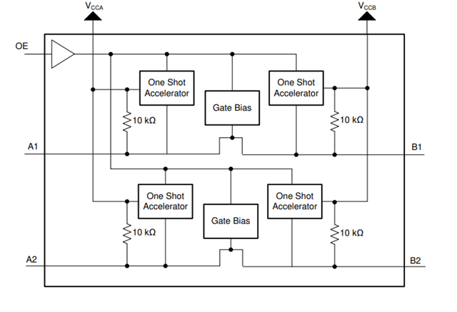
    For sure. They are similar level translators in that they are both passive devices and do not buffer I2C/I3C signals. They differ in that TXS has internal 10k PU resistors on both sides of the device as well as rise-time accelerators on both the input and output for faster rising edges. 

    TCA39306 is purely passive and requires external pullups on the both sides of the device for it to work. See the internal structures from the block diagrams below: 

    TCA39306: 

    Not shown in TCA39306, there are passFET's connecting SDA1 to SDA2 and SCL1 to SCL2. 

    TXS0102: 

    Also, when used as a latch-up countermeasure between an RTC operating on a backup power supply and a device operating on the microcontroller's power supply, which level shifter would be more appropriate?
    May I have more detail to this scenario? What do you mean by "latch-up countermeasure." 

    Are the level translators being powered up at a different time than the MCU? I don't think I understand the full context of the application. 

    Regards,

    Tyler

  • Thank you so much, Tyler.

    Sorry, let me change my question.
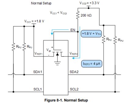
    According to the datasheet, when the OE pin is Low and either VCCA or VCCB power supply is turned off, all outputs become high-impedance.
    In that case, what happens to the input/output pins when the OE pin is High and either VCCA or VCCB power supply is turned off?
    Regards,
    Keita

  • Hi Keita, 

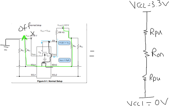
    In the case you described, OE = HIGH, VCCA or VCCB = OFF, then you will get a voltage divider. 

    Please let me know if this makes sense. 

    The opposite is true if VCCA = ON and VCCB = OFF. Then the current will flow from VCCA into the VCCB powered off supply while OE=HIGH. 

    Regards,

    Tyler

  • Hi Tyler,

    Thank you for your response.

    How about the TXS0102? Does the VCC isolation function work?

    I have a question about the TXS0102-Q1 (including TXS0101-Q1).
    Side A is connected using open-drain configuration.
    Since the input/output ports enter a high-impedance state when the power is turned off,
    I am considering adding a 1kΩ pull-down resistor to side B.

    In this case, I am concerned that the high-level voltage on side B may drop during normal operation (when both sides are powered on).
    How should the minimum output high voltage (VOH(min)) on side B be calculated?
    Is the calculation using VCCB × 0.67 correct?


    Regards,
    Keita

  • Hi Keita,

    For VCC isolation / separation, you need to consider using an I2C buffer like TCA9517 / TCA9517A / TCA9617B (recommended). 

    TCA9617B has dual supplies for VCCA and VCCB. The device internal buffer drivers are disabled until both supplies are powered up. 

    What voltages do you need to level translate? 

    Regards,

    Tyler