This thread has been locked.

If you have a related question, please click the "Ask a related question" button in the top right corner. The newly created question will be automatically linked to this question.

DS90CF366: Convert LVDS video data to parallel TFT-Panel data

Part Number: DS90CF366
Other Parts Discussed in Thread: DS90CF386, DS90UB925Q-Q1

Tool/software:

Dear TI-Team,

we want to convert video data from LVDS to parallel, using an interface to deserialize LVDS.

The CPU support video format "RGB888" and "RGB666".

The CPU supports "LVDS JEIDA" and "LVDS VESA" data mapping (LVDS: 4x Data lanes+ 1xClk lane).

We want to use the video format  "RGB666" and "LVDS JEIDA" format.

My questions:

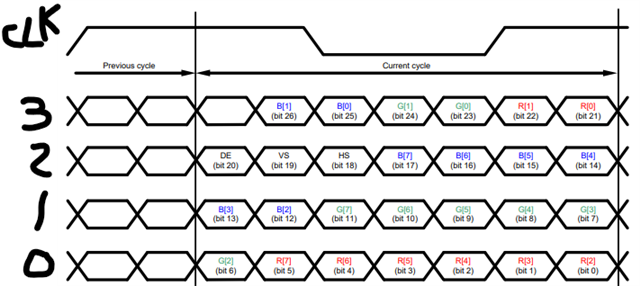
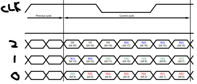
a.) Could we use the part "DS90CF366" (LVDS: 3x Data lanes +1xClk lane), 

to convert CPU video data (RGB666 / LVDS JEIDA) to parallel TFT-panel data (RGB666).

b.) Can you suggest an interface part for converting CPU video data (RGB666 / LVDS JEIDA) to parallel TFT-Panel data (RGB666).

Regards

  • Hi Horst,

    Happy to provide support on this matter. In order for me to provide the most appropriate recommendation, can you please provide me with the full video timings (including active and blanking parameters)?

    Best,

    Nikolas

  • Hello Nikolas,

    attatched is the timing for the TFT-Display (RGB888).

    In this case we use the TFT-Display as RGB666.

    (Reason: OSM-Standard supports only RGB666)

    TFT-Display

    Thank you for helping.

    Regards

  • Hi Horst,

    Thanks for providing additional context. If you are looking for a single-chip solution, I would suggest the DS90CF386 instead of the DS90CF366, since the 386 supports 4 LVDS inputs, whereas the 366 only supports 3 LVDS inputs. As described above, it looks like your CPU has 4 LVDS outputs.

    Alternatively, a DS90UB925Q-Q1 or DS90UB927-Q1 serializer can be utilized in conjunction with a DS90UB926-Q1 deserializer to accomplish the same thing.

    Best,

    Nikolas

  • Thank you for answer that helps a lot.

    Ok than we can use the DS90CF366 (3x LVDS) or DS90CF386 (4x LVDS).

    I habe an additional question:

    In the datesheet for the DSCF366 / DSCF 386 (Page 12 +13) is a "Mapping figure (Figure8 + Figure-9).

    The MAPPING for "DS90CF366 Mapping" is in a logical order and good to understand.

    DS90CF366 Mapping (3xLVDS):

    RxIN0::  RxOUT6    / RxOUT5   / RxOUT4  / RxOUT3   / RxOUT2    / RxOUT1   / RxOUT0

    RxIN1::  RxOUT13 / RxOUT12 / RxOUT11 / RxOUT10 / RxOUT9    / RxOUT8   / RxOUT7

    RxIN2::  RxOUT20 / RxOUT19 / RxOUT18 / RxOUT17 / RxOUT16 / RxOUT15 / RxOUT14

    The MAPPING for the DS90CF386 (4xLVDS) is not so good to understand.

    DS90CF386 Mapping (4xLVDS):

    RxIN0::  RxOUT7   / RxOUT6    / RxOUT4  / RxOUT3   / RxOUT2   / RxOUT1  / RxOUT0

    RxIN1::  RxOUT18 / RxOUT15 / RxOUT14 / RxOUT13 / RxOUT12 / RxOUT9  / RxOUT8

    RxIN2::  RxOUT26 / RxOUT25 / RxOUT24 / RxOUT22 / RxOUT21 / RxOUT20 / RxOUT19

    RxIN3::  RxOUT23 / RxOUT17 / RxOUT16 / RxOUT11 / RxOUT10 / RxOUT5  / RxOUT27

    Question:

    For the DS90CF366 (3xLVDS) is the MAPPING in a following order and clear for me.

    For the DS90CF386 (4xLVDS) is the MAPPING in a transposed order. That is a little bit puzzling to me.

    I do not understand why the order is transposed for DS90CF386 (4xLVDS)

    There must be a reason for that.

    Is this transposed order (DS90CF386(4xLVDS)) also important if we only convert CPU-Video LVDS dataout  to parallel?

    I hope you can help me to understand the difference in MAPPING between DS90CF366(3xLVDS)  and DS90CF386 (4xLVDS).

    Thank you.

    Regards

  • Hi Horst,

    I'm not fully following the difference between the two - the order between Figure 8 and Figure 9 does not look to be transposed. Could you possibly clarify?

    For more details regarding bit mapping, please refer to "Section 8.2.2.3 - Data Mapping between Receive and Endpoint Panel Display."

    Best,

    Nikolas

  • Hello Nikolas,

    i try to explane my issue.

    The two ICs DS90CF366 (3x LVDS) and DS90CF386 (4xLVDS) are different in the bit sequence from LVDS to RGB.
    See data sheet (DS90CF366, DS90CF386) page 12 and 13.

    Figure 8 shows the DS90CF386 mapping of 28 LVCMOS parallel data to serial LVDS data (4xData +1xClk).

    Figure 9 shows the DS90CF366 Mapping of 21 LVCMOS parallel Data to serial LVDS Data (3xData +1xClk).

    It is a bit confusing because the parallel bits from both ICs (DS90CF366, DS90CF386) are present at different positions in the serialized LVDS stream.

    For example, serialized bit sequence for LVDS line “RxIn0”.

    DS90CF366/RxIN0:
    RxOut0, RxOUT1, RxOUT2, RxOUT3, RxOUT4, RxOUT5, RxOUT6 / .....

    DS90CF386/RxIN0:
    RxOut0, RxOUT1, RxOUT2, RxOUT3, RxOUT4, RxOUT6, RxOUT7 / .....

    My Question:

    If I understand it correctly, the deserialized bits for the display (RGB888) of the DS90CF386 must be connected (in schematics)

    according to "Datasheet DS90CF386/Sectiob 8.2.2.3.

    For example "Table 2 (8-Bit Color Mapping on RxIN3)" .

    Regards

    Horst

  • Hi Horst,

    I see the confusion now - the two devices have two separate bit mappings. For added context, please refer to the following statement from the data sheet:

    The reason why RxOUT# is not perfectly sequential in Figure 8 is because for DS90CF386 RGB666 applications, the LSBs for each color are placed on RxIN3 so that they are easier to be left as NC (so that only one LVDS input channel that houses all three LSBs needs to be left as NC instead of one stream position across three separate LVDS input channels). See the following timing diagram with MAPSEL = L for details (note that this is from a 92x data sheet, but the same principles apply):

    For Figure 9 and DS90CF366 RGB666 applications, RxIN3 does not exist, so therefore the RxOUT# pins are mapped sequentially. See below timing diagram with MAPSEL = L (again, note that this is from a separate data sheet but the same principles apply):

    It also looks like Table 2 and 3 for DS90CF386 slightly groups RxIN# and RxOUT# incorrectly. Please note that each RxIN# should correspond with 7 RxOUT#s.

    Best,

    Nikolas