Other Parts Discussed in Thread: ADS131M04
Tool/software:
Dear team,
I have connected 2 ADS131 evm board (with external supply) to MCU over same SPI lines(MISO, MOSI, SCLK). DRDY & CS for both ADCs connected to separate GPIOs.
OSR I have kept 512 (8Ksps),
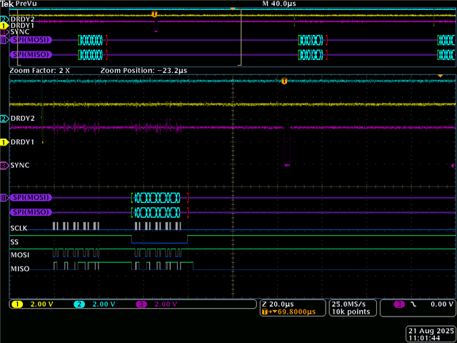
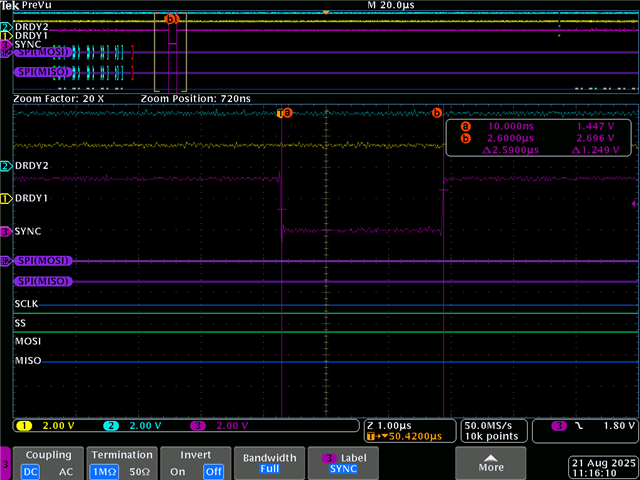
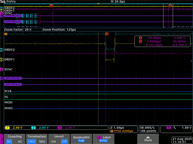
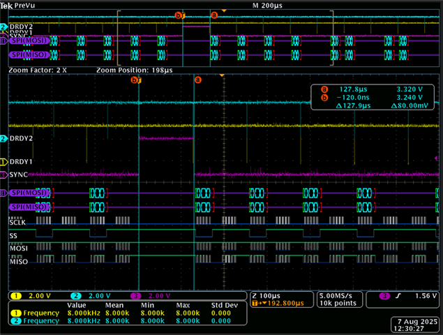
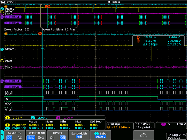
Once i toggled the Sync pin, both ADCs are in sync, but after some period both ADCs are slowly coming out of sync. I am monitoring DRDY signal of both adc & below i have attached the screenshot once sync is toggled & after 1minute of sync.
1. Once sync is toggled
2. After a minute, shift between both DRDY is ~4.5us.
If this behaviour is common, then at what rate we need to sync the device?
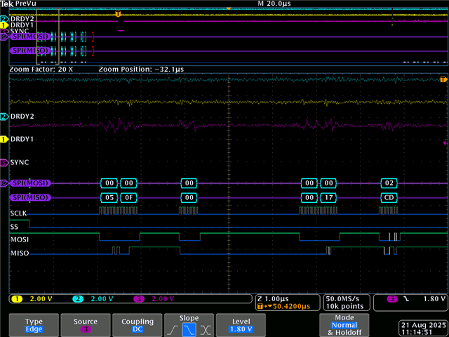
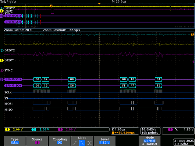
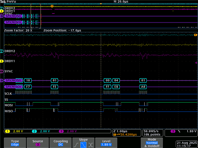
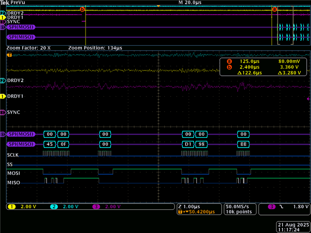
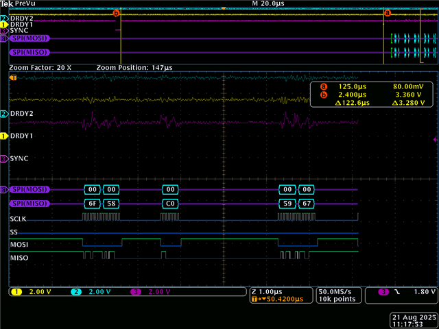
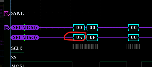
Also I have seen once sync is done, the next response which i get on both adc is varying sometimes. This i checked on multiple trials of sending the sync signal. RESET bit & REG_MAP bit sets in STATUS register, even if ADC is not resetted or reset signal is not given.
Regards,
Shraddha