MAX3243E: MAX3243ECDBR Circuit Connection and V+ Pin Miswiring

Guru 12115 points
Part Number: MAX3243E

Tool/software:

Hi,

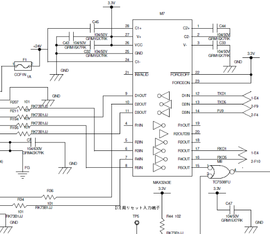
I would like to consult about a circuit using the MAX3243ECDBR.

We implemented the attached circuit and observed the following issues:

  • Even when applying a valid TTL signal to pin 13 (T2IN), no RS-232 level signal was observed at pin 10 (T2OUT).

  • When we tested with 3.3V connected to the V+ pin, the IC was damaged.

According to the datasheet (MAX3243E recommended circuit), I understand that V+ and V– are generated internally by the charge pump and should not be externally powered. However, in our circuit it seems we mistakenly connected 3.3V to V+.

Could you please confirm the following points?

  1. Is it correct that applying an external supply to V+ is likely to cause device failure?

  2. Should the capacitors for C1+/C1– and C2+/C2– be placed directly between the respective pins, and not to ground?

  3. Are there any cases where alternative connections (different from the datasheet’s recommended circuit) are acceptable for proper operation?

We would appreciate your confirmation.

Best regards,

Conor

  • Is it correct that applying an external supply to V+ is likely to cause device failure?

    Yes, the device was not designed or intended to be connected to a power supply rail here. 

    Should the capacitors for C1+/C1– and C2+/C2– be placed directly between the respective pins, and not to ground?

    Yes, correct. Those are the charge pump caps that are used to generate a larger voltage onto the V+ and V- pins.

    Are there any cases where alternative connections (different from the datasheet’s recommended circuit) are acceptable for proper operation?

    Sometimes, you can connect the V+ cap to Vcc instead of GND. A side from this, I would not recommend any other alternative connections.

    -Bobby

  • Hi Bobby,

    Thank you for your feedback.
    Is there anything you're concerned about with the following circuit?

    The V+ and V- of the MAX3243E are the output terminals of the internal charge pump, not the point where an external power supply is applied.

    V+ is defined as the "positive charge pump output voltage," and V- is defined as the "negative charge pump output voltage." Could connecting an external 3.3V to V+ damage the device?

    Also, the charge pump capacitors are connected directly between C1+ and C1- and between C2+ and C2-. Reservoir capacitors (C3 and C4) are connected to V+ and V- between V+ and GND, respectively. I believe the recommended values ​​for C1 through C4 are 0.1µF when operating at 3.3V.

    Best regards,

    Conor

  • V+ is defined as the "positive charge pump output voltage," and V- is defined as the "negative charge pump output voltage." Could connecting an external 3.3V to V+ damage the device?

    I actually do not know if this is guaranteed to cause damage. This pin is meant to store the charge that the charge pumps build up. When you place a voltage rail on this (and its lower than the intended voltage) the charge will not be able to build up and leak into the supply. I suspect there is also some kind of circuit that verifies if the charge pumps are working and will disable the device if they are not. I do not know if that feature would protect the device from damage though.

    Is there anything you're concerned about with the following circuit?

    Is there actually a 24V rail tied directly to C1-?

    This looks like it would definitely break the device. 

    -Bobby