SN65LVDS32: SN65LVDS32DR G̅ Pin Not Deactivating Chip Outputs

Part Number: SN65LVDS32

Tool/software:

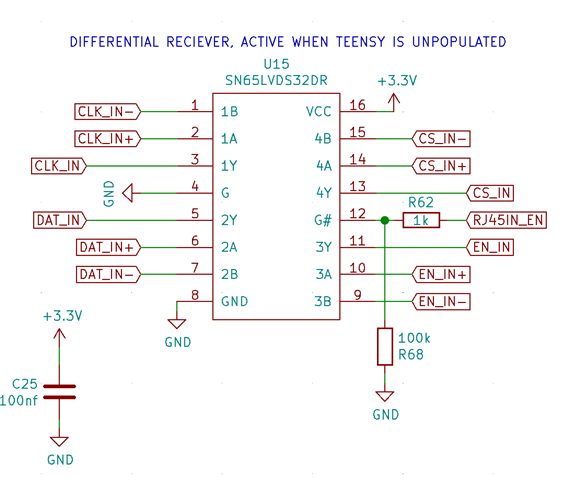
Hi, I am dealing with an issue on my design using the SN65LVDS32DR where driving the enable (active low) pin G̅ into a high state does not disable the chip outputs and set them to a high Z state. 

My supply voltage is 3.3V and I have checked with a scope that 3.3V is present on the G̅ pin 12, but the outputs are still active, causing them to fight with another digital signal driver. 

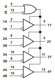
Here is the relevant portion of my schematic:


I write RJ45IN_EN high with a micro pin to disable the SN65LVDS32DR chip (so the micro can provide these signals instead) but even with the micro pin holding G# (pin 12) at 3.3V the outputs are still fighting with my micro output (shows up as voltage drop and noise). The issue does not go away until I physically remove the SN65LVDS32DR from the board. 

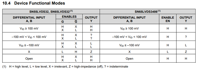
Pleaes advise on what is going wrong here, this seems to directly contradict the behavior described in the datasheet. 

Thanks!

  • Hi Emmett,

    Thanks for reaching out. This is because you are constantly holding the G pin high. If you look at section 10.2 if the datasheet (below) you'll see the G and /G are ORd together, so if G is pulled high, the output of that OR gate will always be high. Connecting the G pin to GND instead of 3.3 V should fix your issue. 

    Regards,

    Matt 

  • Ah, so disable is an AND and enable is an OR. The written description of the pin functionality in the datasheet makes it sound like the opposite which is how I was trying to use it. 

    Maybe this could be made more clear, would have saved a lot of time. 

    Thanks for the resolution. 

  • To clarify, if I want to have the chip disabled by writing a single pin high, can I just connect G to ground and G̅ to gpio logic?

    New schematic here (RJ45IN_EN connects to the micro pin):

  • Please refer to the table below. If G is high OR if /G is low, the output of the device will be enabled regardless of the opposite pin's state. If G is low AND /G is high, the output will be disabled and go high impedance.  Your schematic is correct. The device output will be enabled by default since /G is pulled low and disabled when RJ45IN_EN drives /G high.