DP83867IR: Question on DP83867IRPAP Circuit Design

Part Number: DP83867IR

Tool/software:

Hello,

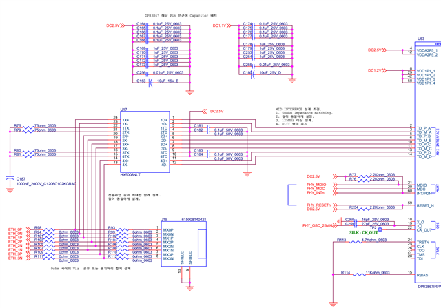
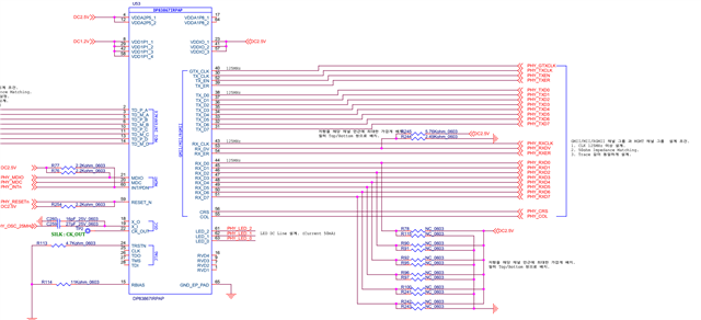
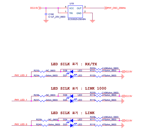
We have completed the circuit design for the DP83867IRPAP as outlined below.

This design is a revision of our existing product, replacing the Marvell 88E1111-BAB with the DP83867IRPAP.

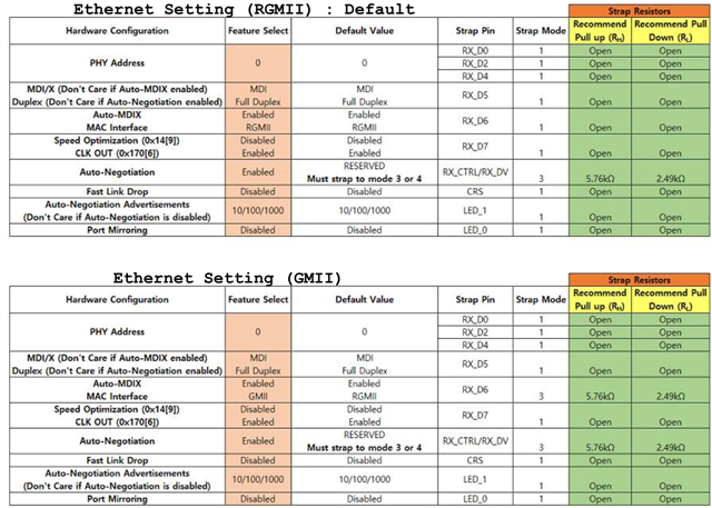
The default STRAP PIN configuration is RGMII. To verify compatibility with the existing FPGA firmware without any modifications, all STRAP PIN resistors have been applied so that the configuration can also be switched to GMII.

We would like to confirm if there are any potential issues or considerations with this configuration.

Thank you for your support.

Best regards,

Jun-Seok, Bae

  • Hi,

    The strapping table looks correct between GMII and RGMII. Any chance you can attach the schematic as a .pdf doc? The resolution is too small to make a proper review of the design.

    Thanks

    David 

  • Hi.

    Since file attachment is not possible, I have divided the circuit into captures and uploaded them.

    Thanks

    JSBae

  • JSBae

    1. I would recommend putting the ESD protection diode between the transformer and DP83867

    2. Please check the VDD1P1 voltage and make sure it meets the DP83867 recommended operating condition

    3. Why do you need two capacitors on the XI input?

    4. Why do you provide 2.5V on the center tap of the transformer? Please do not short the center tap together.

    5. You need to have a earth ground on the transformer and RJ45 side

    6. Can you add a 1uF pulldown capacitor on the RESET?

    Thanks

    David

  • 1. I would recommend putting the ESD protection diode between the transformer and DP83867

         - I will keep it in mind.

    2. Please check the VDD1P1 voltage and make sure it meets the DP83867 recommended operating condition

         - It has been configured to meet the conditions.

    3. Why do you need two capacitors on the XI input?

         - When using a 3.3V~2.5V oscillator, this is a recommended requirement in the datasheet. The oscillator currently in use is for 2.5V. Is there anything incorrect?

    4. Why do you provide 2.5V on the center tap of the transformer? Please do not short the center tap together.

          - I will reflect the configuration so that it is separated by resistors.

         - As an additional inquiry, we have been using the current transformer configuration without any issues so far.

         - Is there a specific reason why the CTs need to be separated? Below is the internal circuit of TE’s 2301997-7 RJ45. All CTs are shorted together. (Used in the FPGA EV-KIT DP83867)


    Circuit modification

    2301997-7 Circuit

    5. You need to have a earth ground on the transformer and RJ45 side.

         - I will keep it in mind.

  • Hi

    3. Why do you need two capacitors on the XI input?

         - When using a 3.3V~2.5V oscillator, this is a recommended requirement in the datasheet. The oscillator currently in use is for 2.5V. Is there anything incorrect?

    Understood, no more question from my side.

    4. Why do you provide 2.5V on the center tap of the transformer? Please do not short the center tap together.

          - I will reflect the configuration so that it is separated by resistors.

         - As an additional inquiry, we have been using the current transformer configuration without any issues so far.

         - Is there a specific reason why the CTs need to be separated? Below is the internal circuit of TE’s 2301997-7 RJ45. All CTs are shorted together. (Used in the FPGA EV-KIT DP83867)

          Each center tap on the side connected to the PHY, must be isolated from one another and connected to ground via a decoupling capacitor (0.1µF recommended). Your current implementation is correct.

    Thanks

    David

  • Hi.

    Thank you for your response. It was very helpful.

    Best regards,

    JSBae.