TUSB4041I-Q1: PCB Via design

Part Number: TUSB4041I-Q1

Tool/software:

Hi,

Let me ask you a basic question about the "Via" design of the PCB design as below.

Regarding the "Vias" in the GND and thermal PAD located beneath of this device,

are ther any design requirements that are considered "mandatory" or "recommended" ?

Especially, "PAD on Via" and "Filled Via" are "mandatory" or "recommended" ?

And your recommend PCB layout is the one which is on the datasheet, right?

The "Vias" which are shown on the datasheet are ”Unfilled Via”, correct?

Thank you for your support.

Best Regards,

Takumi

  • Hi,

    Sorry let me ask you an additional following question, please.

    My customer is currently experiencing poor soldering on the power pad for this device (occurrence rate: approximately 1%).

    It's possible that solder has flowed into the via, causing insufficient soldering on the thermal pad.

    Is the relationship between the stencil and the stencil opening a possible factor in this defect? ​​

    Also, does the number of vias play a role? The customer used an older datasheet as a reference for their design.

    The number of vias is fewer than in the latest datasheet. (The latest version has 8x8=64 vias, while the customer's design has 6x6=36, with a pin spacing of 1.3mm.)

    Currently, hollow vias are used, but we are considering changing them to filled vias or other options.

    We would also like to consider the relationship between the stencil and the opening, if that is also a factor.

    I would appreciate any advice on this matter.
    Thank you in advance.

    Best Regards,

    Takumi

  • Let me inform you the additional information about the PCB.

    The PCB is made of FR-4 and is a six-layer board.

    Thanks again!

    Takumi

  • Hi Takumi:

      We do recommend PCB layout is the one which is on the datasheet, but not  mandatory .

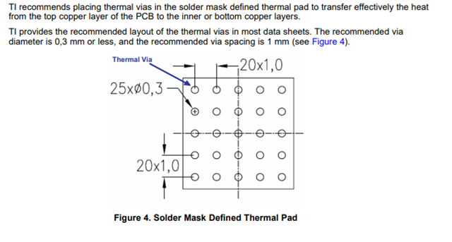
    The recommended via diameter is 0,3 mm or less, and the recommended via spacing is 1 mm

       Or customer can use example of TUSB4041EVM layout since  it was proving working layout.

    Regards

    Brian

  • For stencil  information, please check  section 4.2 of  this document of this document.

    QFN and SON PCB Attachment (Rev. C) 

    Best

    Brian