Tool/software:


Please explain in detail how to configure this mode. Thank you!
Hi Tony,
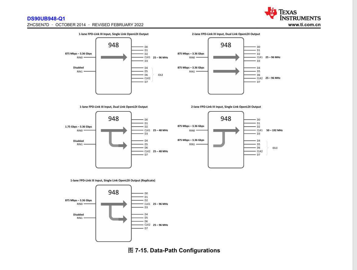
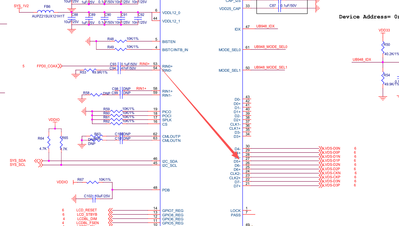
This should be possible with OLDI Port 1 and Port 0 active to achieve the diagram you have shown where RIN0 > D4-D7.
The replicate feature should be employed here, as the content coming into RIN0 will be replicated at both Port 0 (unused) and Port 1.
Depending on the MAPSEL you will need for the timing configuration, this will either be No. 3 or No. 7.


Reminder of MAP_SEL modes are shown below:


Please let me know if you have any questions!
Best,
Miguel
Hi Liguo,
Register 0x34 refers to the RX mode on the 948. Is there a serializer sending video through the FPD-Link at this time?
Can you please provide a block diagram and a register dump of the system to confirm the settings?
For register 0x49:
7 = MAPSEL = H
6 = MAPSEL overwrite enabled
5 = MAPSEL overwrite = H
4-2 = Reserved
1-0 = Replicate FPD-OLDI Output
Best,
Miguel