Part Number: SN65DP159
Tool/software:
Dear TI Support team,
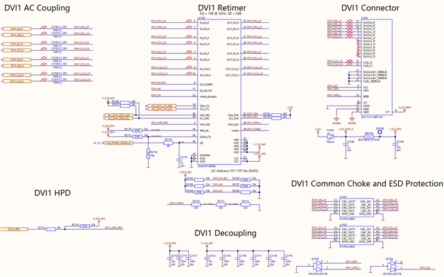
1. The issue description: in our application, we have two DVI(HDMI1.4) outputs using two SN65DP159RSB retimer. the schematic design is exactly same and the PCB layout is basically same and adjcent placed. Hereinafter referred to as DVI1 and DVI2. Basically the DVI1 and DVI2 were operated same time, after one period normal operation, the DVI1 output abnormal(no display on some or most monitors) while DVI2 still good. Among a total of about 20 products, 4 cases were found.
2. The debugging I have did
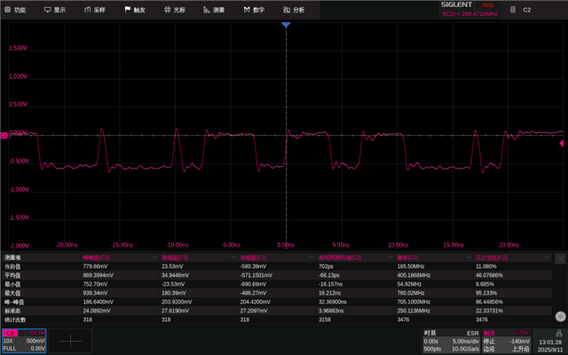
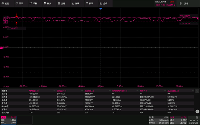
i. Compare the DVI1 and DVI2, the inputs signals are same but the outputs of DVI1 are abnormal, as screenshots as below
DVI2 outputs (OUPUT_D2), differential signals, normal
DVI2 outputs (OUPUT_D2_P), single mode signals, the OUTPUT_D2_N is similar
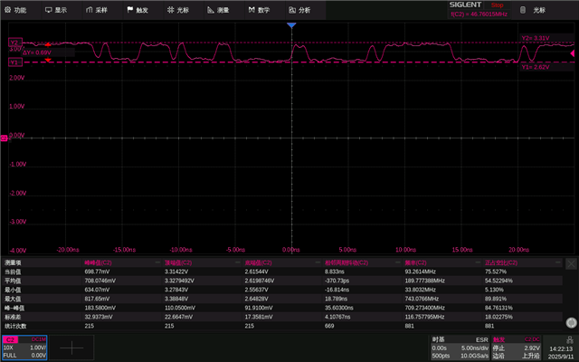
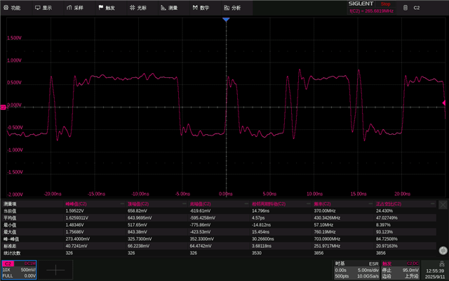
DVI1 outputs (OUPUT_D2), differential signals, abnormal
DVI1 outputs (OUPUT_D2_P), single mode signals, the OUTPUT_D2_N is similar
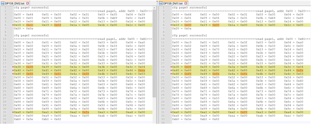
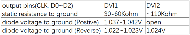
ii. Compare the DVI1 and DVI2, the static measurements as below
iii. Rework to replace the DVI1's retimers chip bty new one, the output signals are normal and the monitor display ok.
iv. It was suspected that the chip failure was caused by ESD. Therefore, ESD tests (Contact/AIR +/-15KV) were conducted on normal output DVI ports for over 1000 times, but the problem did not recur.
v. Possible doubts, the DVI1's circuity is close heat source - the FPGA module's heat sink, but i measured the air temperature is under 50℃, while the operation temperature of SN65DP159RSB is -40~85℃.
3. My questions/requests
i. Why there is different failure rate for same design? 1/5 for DVI1 but 0 for DVI2.
ii. Find the root cause and then guide for design optimization.
4. design inputs for review
i. Firmware: I2C config but completely default settings
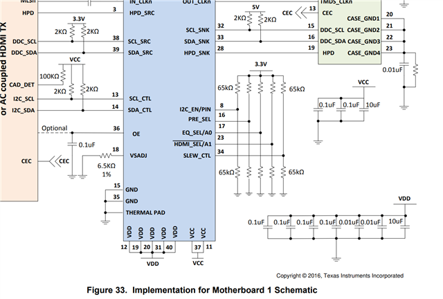
ii. Schematic
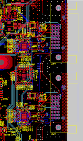
iii. Layout