SN65DSI86: *ERROR* Link training failed, link is off (-5)

Part Number: SN65DSI86
Other Parts Discussed in Thread: TS3DV621

Tool/software:

Hello,

We use the SN65DSI86 for a two-lane eDP connection. With our 15.6” FHD colour TFT-LCD display, the training link fails and we get a blank screen after 3 to 5 power cycles. The display is two-lane compatible and has a data rate of 2.7 Gbps per lane. If we reboot it, in most of the cases the next training link is successful but the problem is still very annoying.

Looking at error registers 0xf0–0xf8 of the SN65DSI86 DSI-to-DP bridge, during a failed cycle the register value is 0x12 (LT_EQ_LPCNT_ERR) instead of the expected 0x01 (Semi-Auto link training successful). This indicates that the link training failed in the channel equalization phase.

Looking at the link training register, if it fails, register `0x93` shows a value of `0xa4`, which means that pre-emphasis level 2 is set.
Register 0x94 shows a value of 0x81, which means voltage swing level 1. In a successful cycle, pre-emphasis and voltage swing are both always level 0.

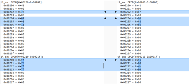
I also read the DPCD of the sink and compared the passing and failing cycles.

According to the DP standard, registers 0x103 and 0x104 set the output voltage and pre-emphasis levels respectively. In a failing cycle, these registers are set to the value `0x30`, which indicates a pre-emphasis level of 2 and that the maximum setting has been reached. This is the same as I could read out before from the bridge.

Left Pass, Righ Fail


Looking further, if it's a pass, I see register 0x202 has a value of 0x77, so CR and channel EQ have been completed and the symbol is locked for lanes 0 and 1.

However, if it fails, the value is `0x17`, meaning that the CR and channel EQ are complete and symbol is locked for lane 0 but lane 1 has the CR complete, but the channel EQ fails.

Registering a value of 0x00 instead of 0x01 in register 0x204 also shows me that interlane alignment was not successful.


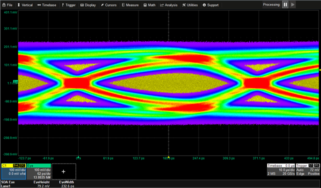
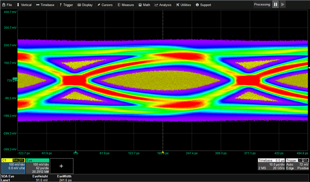
This all would point to a signal integrity issue in the main link, probably on lane 1, but looking at lane 0 and 1 the eye seems to be good enough. The measurement was done directly on the eDP connector.

channel 0:

channel 1:

Any ideas?

kind regards

Franz

  • Hi Franz,

    Could you give us a description of the test setup. Is this the TI EVM or custom board? Is the DSI86 bridge and DP receiver on the same board or is there a connector and cable?
    It would help to know whether there is an SI issue. Are the used DP lanes length matched?

    If you have another DP receiver available, could you test the device and check if it also has link training issues. This would be if it's possible to connect to a different receiver and display.

    Best regards,
    Ikram

  • Hey Ikram,


    Could you give us a description of the test setup. Is this the TI EVM or custom board? Is the DSI86 bridge and DP receiver on the same board or is there a connector and cable?
    It would help to know whether there is an SI issue. Are the used DP lanes length matched?

    It's an SoM to carrier board concept. The DSI86 bridge is located on the SoM and connected to the eDP connector on the carrier. The distance between the two is around 230 mm in PCB. Then, we use a 30-pin cable around 20 cm long to connect to the display.
    Between the SoM and the eDP connector, there is a TS3DV621RUAR mux to select for DP or eDP. DP shows no issues at all, and we were able to test it with different sinks, but there we also use four lanes instead of two.
    The lanes are length matched.

    We're also trying to get another eDP display for testing but I saw that there are a few similar posts in the forum, so it would be important to know if there are any limitations we should consider in our design.

    Thanks

    Franz

  • Hi Franz,

    1. Could you please tell us what the DSI clock and data rate is for this resolution? You will find in the datasheet that there are limitations on maximum clock and data rates per lane.

    2. Is the system working currently with 4 lane DP output output not working with 2 lane DP? Is this tested and confirmed with this same setup?

    3. Could you also please get a register dump of the DSI86 device. It would especially help to check the 0xF0 - 0xF8 registers.

    Best regards,
    Ikram

  • Hi Ikram,

    I'm jumping in since Franz is on vacation. Please find the answers below:

    1. The clock rate is 142 MHz while the data rate is 2.7 Gbps, both not exceeding the maximum possible values. The screen we use is the G156HAN03.0.

    2. The 4 lanes DP output does work fine but the 2 lanes eDP output is the one which is failing from time to time. The output is selected with a TI MUX TS3DV621.

    3. I attached two register dumps, one for a working output and one for a failing output. Regarding 0xF0 - 0xF8: 0xF8 had different values from time to time if the output fails. It's either 0x12 or 0x0A

    i2cdump_working_run
    
         0  1  2  3  4  5  6  7  8  9  a  b  c  d  e  f    0123456789abcdef
    00: 36 38 49 53 44 20 20 20 02 00 86 00 00 01 00 00    68ISD   ?.?..?..
    10: 26 00 55 00 00 00 00 00 00 00 00 00 00 00 00 00    &.U.............
    20: 80 07 00 00 38 04 00 00 00 00 00 00 30 80 00 00    ??..8?......0?..
    30: 0a 80 00 00 18 00 1a 00 6c 00 0a 00 00 00 00 00    ??..?.?.l.?.....
    40: 51 43 00 00 80 00 34 08 66 04 48 00 24 00 30 80    QC..?.4?f?H.$.0?
    50: 0a 80 80 07 38 04 20 00 40 1b 0d 00 11 00 30 00    ????8? .@??.?.0.
    60: a0 60 a4 00 00 00 00 00 00 00 00 00 00 00 00 00    ?`?.............
    70: 00 00 00 00 00 01 02 01 80 81 00 31 35 36 48 41    .....?????.156HA
    80: 4e 30 33 2e 30 20 0a 00 bb 1f 7c f0 c1 07 1f 7c    N03.0 ?.??|????|
    90: f0 c1 07 24 80 00 01 04 01 00 00 00 00 00 00 00    ???$?.???.......
    a0: 01 ff ff 00 00 00 00 00 00 00 00 00 00 00 00 00    ?...............
    b0: 04 78 ac ac 08 6c 9c 9c 0c 5c 5c 5c 0c 0c 0c 0c    ?x???l???\\\????
    c0: 3f 3f 0f 00 00 00 00 00 00 00 00 00 00 00 00 00    ???.............
    d0: 00 00 00 00 00 00 00 00 00 00 00 00 00 00 00 00    ................
    e0: 00 00 00 00 00 00 00 00 00 00 00 00 00 00 00 00    ................
    f0: 00 00 00 00 01 00 00 01 01 00 00 00 00 00 00 00    ....?..??.......

    i2cdump_failing_run
    
         0  1  2  3  4  5  6  7  8  9  a  b  c  d  e  f    0123456789abcdef
    00: 36 38 49 53 44 20 20 20 02 00 06 00 00 00 00 00    68ISD   ?.?.....
    10: 26 00 55 00 00 00 00 00 00 00 00 00 00 00 00 00    &.U.............
    20: 00 00 00 00 00 00 00 00 00 00 00 00 00 00 00 00    ................
    30: 00 00 00 00 00 00 00 00 00 00 00 00 00 00 00 00    ................
    40: 00 00 00 00 80 00 00 00 00 00 00 00 00 00 00 00    ....?...........
    50: 00 00 00 00 00 00 20 00 40 1b 05 00 11 00 30 00    ...... .@??.?.0.
    60: a0 60 a4 00 00 30 00 00 00 00 00 00 00 00 00 00    ?`?..0..........
    70: 00 00 00 00 00 01 02 01 80 17 00 31 35 36 48 41    .....?????.156HA
    80: 4e 30 33 2e 30 20 0a 00 bb 1f 7c f0 c1 07 1f 7c    N03.0 ?.??|????|
    90: f0 c1 07 a4 80 00 00 04 01 00 00 00 00 00 00 00    ?????..??.......
    a0: 01 ff ff 00 00 00 00 00 00 00 00 00 00 00 00 00    ?...............
    b0: 04 78 ac ac 08 6c 9c 9c 0c 5c 5c 5c 0c 0c 0c 0c    ?x???l???\\\????
    c0: 3f 3f 0f 00 00 00 00 00 00 00 00 00 00 00 00 00    ???.............
    d0: 00 00 00 00 00 00 00 00 00 00 00 00 00 00 00 00    ................
    e0: 00 00 00 00 00 00 00 00 00 00 00 00 00 00 00 00    ................
    f0: 00 00 00 00 01 20 00 00 12 00 00 00 00 00 00 00    ....? ..?.......

  • Hi Janick,

    In the working runs, where link training is successful, is video output also successful on display?

    Is there any issue with the DP signal path with MUX and other connections that could be an issue here? If link training is failing, you could also try fast link training or manual link training to see if it works consistently.

    I will look into the register dumps further and get back to you.

    Best regards,
    Ikram


  • Hi Janick, 

    Were you able to get successful display or test with fast link training?

    Based on the register dumps, is there valid REFCLK input for both working and not working cases? Also, please try enabling the 0xD register DP_PLL_EN bit as shown in the initialization step 12. Could you please check whether the init sequence is followed throughout.

    Best regards,
    Ikram

  • Hey Ikram

    If the link training is successful I get a working output on the display. I was not able to try the fast link training yet since it requires us to build a new image. Triggering the semi auto link training after it failed initially (writing 0x0A into register 0x96) does not resolve the issue. 

    The 0x0D register is set by the driver, if the link training fails. That's why it is 0 for the failing register dump.

    /* Disable the PLL if we failed */
    	if (ret)
    		regmap_write(pdata->regmap, SN_PLL_ENABLE_REG, 0);
    
    	return ret;

  • Hi Janick,

    The initialization sequence mentions "The SN65DSI86 only supports ASSR Display Authentication method and this method is enabled by default"

    Does the DP sink have ASSR support? Since it is not working in eDP mode, please check this and state of DP register address 0x0010A.

    Best regards,
    Ikram