DS90CR287: DS90CR287 PLL Problem

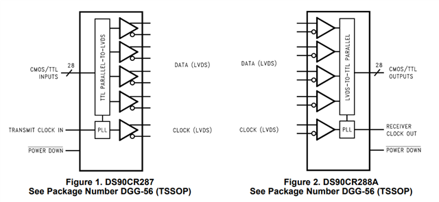
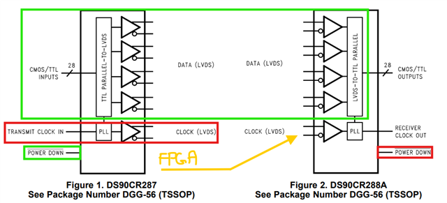
Part Number: DS90CR287
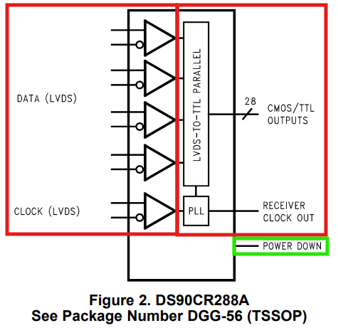
Other Parts Discussed in Thread: DS90CR288A,

Tool/software:

Hi everyone,

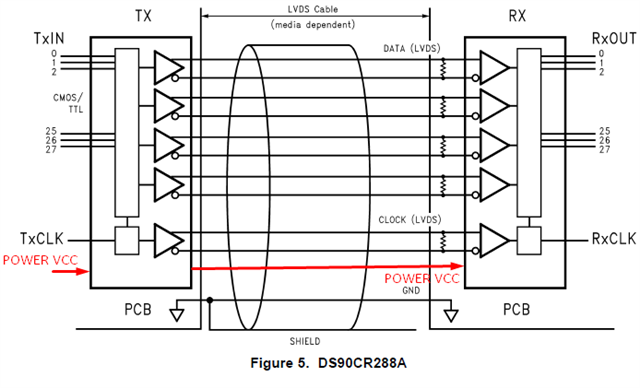
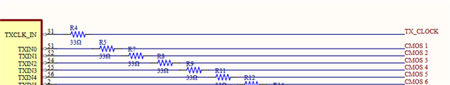
I have DS90CR287 for TX and DS90CR288A for RX chips. I tested before these chips (first power up) and i get clock and data with little noise. Design has decoupling capacitor. Then second power up i can not get any clock from TX side. I give diff clock with FPGA to RX chip, it is worked. Problem is TX side. My boot up sequence is below:

  1. TX power up ( PWRDWN is low)
  2. FPGA power up and give clock same time.
  3. TX PWRDWN is high.

So reference guide and other thread what i read , telling me this seqeuence. But i can not get any clock second power up section. Is it about chip or PLL? All voltages is 3.3 and ground is connected. (PLL,LVDS and VCC ext.) I changed IC 3 times and same results i get.

Thanks for reply.

Best regards,

  • Hi Samet,

    Let me summarize the information above,

    Upon first power up, the sequence is:

    DS90CR287 Power Up, no signal applied to TX PWR_DOWN_B -> FPGA Power up and provide clock to DS90CR287 at the same time -> Enable TX PWR_DOWN_B = HIGH

    Will be referencing APPLICATIONS INFORMATION of our data sheet, specifically TRANSMITTER INPUT CLOCK and POWER SEQUENCING AND POWERDOWN MODE.

    DS90CR287/DS90CR288A 3.3V Rising Edge Data Strobe LVDS 28-Bit Channel Link 85MHz datasheet (Rev. G)

    According to the data sheet sequence, this should be valid.

    Let me ask a few clarification questions:

    When you power cycle the device and bring it back up again, what is the exact power sequencing for each device?

    • FPGA with provided CLK
    • TX DS90CR287
    • RX DS90CR288

    My assumption is that depending on how the power cycling is done for the pair of devices, the RX device might be in a lock-up state, please see the attached information from the data sheet:

    "The CHANNEL LINK chipset is designed to protect itself from accidental loss of power to either the transmitter or receiver. If power to the transmit board is lost, the receiver clocks (input and output) stop. The data outputs (RxOUT) retain the states they were in when the clocks stopped. When the receiver board loses power, the receiver inputs are shorted to VCC through an internal diode. Current is limited (5 mA per input) by the fixed current mode drivers, thus avoiding the potential for latch-up when powering the device."

    For the transmitter input clock these are the requirements:

    The transmitter input clock must always be present when the device is enabled (PWR DOWN = HIGH). If the clock is stopped, the PWR DOWN pin must be used to disable the PLL. The PWR DOWN pin must be held low until after the input clock signal has been reapplied. This will ensure a proper device reset and PLL lock to occur.

    This is unlikely to be the issue, but we can further analyze the sequencing between power cycles to understand if all requirements are being met at the TX.

    You could attempt to reset the PLL after the second power cycle, by disable PWR_DOWN_B = LOW then enable PWR_DOWN_B = HIGH.

    Please let me know if you have this additional information.

    Thanks,

    Miguel

  • Hi Miguel,

    First i tried this, there is no RX connection.

    1- FPGA no power up, bitstream is ready with clk. When i power up, it will be out from pins to TX pin. TX has no power this time.

    2- TX is power up but PWR_DWN(32. Pin) is thorugh to GND (pull down). Chip has 3.3V each VCC, PLL_VCC and LVDS_VCC pin. (I make toggle different time same scenerio btw)

    3- Then TX_PWR_DWN is going to HIGH. (pull-up). Chip has TX CLK_IN but there is no CLK_OUT.

    Same scenerio, with RX connection, when i TX_PWR_DWN is pull up, RX chip is PWR_DWN pulldown but has power. Then i pull up RX_PWR_DWN. I tried all scenerio i guess. RX and TX has same GND and VCC source btw.

  • Hi Samet,

    1- FPGA no power up, bitstream is ready with clk. When i power up, it will be out from pins to TX pin. TX has no power this time.

    First FPGA is powered on, then sending CLK signal and data signal to the input of the TX:

    At this time, the DS90CR287 is not powered at all.

    2- TX is power up but PWR_DWN(32. Pin) is thorugh to GND (pull down). Chip has 3.3V each VCC, PLL_VCC and LVDS_VCC pin. (I make toggle different time same scenerio btw)

    DS90CR287 is enabled, but the POWER_DOWN is still pulled low.

    3- Then TX_PWR_DWN is going to HIGH. (pull-up). Chip has TX CLK_IN but there is no CLK_OUT.

    Finally, POWER_DOWN is pulled HIGH but there is no output on the PLL for CLOCK (LVDS) (assuming this is measured on a waveform).

    Same scenerio, with RX connection, when i TX_PWR_DWN is pull up, RX chip is PWR_DWN pulldown but has power. Then i pull up RX_PWR_DWN.

    I will consider this step 4, so now DS90CR288 is powered on, initially off, then enable through POWER_DOWN pulled high.

    So this is only on the second power cycle of the devices, let me try to understand the flow:

    I tested before these chips (first power up) and i get clock and data with little noise.

    Initially it is working end-to-end on first power up.

    Then second power up i can not get any clock from TX side. I give diff clock with FPGA to RX chip, it is worked.

    So on second power-up, the clock from the FPGA is directly transferred to the DS90CR288 CLK_IN, but where is the data (CMOS / TTL) inputs coming from? Still the FPGA -> TX -> RX?

    On the second power cycle, I am trying to understand if the following steps are being taken:

    1. Whole system is ON (following the sequence described earlier), there is video end-to-end with clock and data and little noise
    2. Whole system is powered OFF, FPGA is powered down, both TX and RX chip VCC has no power.
      -
    3. Initialize and send video from FPGA (data and clock to input of TX device)
      -
    4. Power on TX device, initially PWR_DWN = LOW
    5. Enable TX device, PWR_DWN = HIGH
      -
    6. Power on RX device, initially PWR_DWN = LOW
    7. Enable RX device, PWR_DWN = HIGH

    Even with the sequence mentioned above, TX output clock LVDS cannot produce any signal?

    Please let me know your feedback.

    Best,

    Miguel.

  • At this time, the DS90CR287 is not powered at all.

    1- No, FPGA has clock but not powered on. First DS90CR287 is power on but PWR_DWN is low. When i give power on FPGA it will give the clock to DS90CR287. Basically;

    FPGA_POWER = OFF , DS90CR287= ONPWR_DWN= LOW

    DS90CR287 is enabled, but the POWER_DOWN is still pulled low.

    2- Yes.

    Finally, POWER_DOWN is pulled HIGH but there is no output on the PLL for CLOCK (LVDS) (assuming this is measured on a waveform).

    3- Yes, exactly.

    I will consider this step 4, so now DS90CR288 is powered on, initially off, then enable through POWER_DOWN pulled high.

    4- 288 and 287 has same power line. When 287 power on, same time  288 has power on too.

    When I pull up PWR_DWN of 287, PWR_DWN of 288 stil LOW.

    FPGA_POWER = ON, DS90CR287= ON, 287_PWR_DWN= ON,   DS90CR288 = ON,  288_PWR_DWN = OFF. For this setup 287 has no LVDS CLOCK OUT.

    Then,

    FPGA_POWER = ON, DS90CR287= ON, 287_PWR_DWN= ON,   DS90CR288 = ON,  288_PWR_DWN = ON.

    STILL NO CLOK OUTPUT 287 AND 288.

    So on second power-up, the clock from the FPGA is directly transferred to the DS90CR288 CLK_IN, but where is the data (CMOS / TTL) inputs coming from? Still the FPGA -> TX -> RX?

    5- No, there is no any data. I only want to check RX chip. I give only diff clock from FPGA to 288 LVDS CLOCK IN. I got same clock from Receiver OUT CLOCK.

    This all conversion of top, i all tried my setup scenerio. Not first boot up.

    On first boot up, i tried to check basic test with FPGA-TX-RX. I got clock with noise from RX side. Then i power off all setup and changed my design from FPGA side,(only data mapping), then i power up with  same scenerio but i got any clock and data  this time. I still getting no data and clock now. I changed IC 4 times. Every time i get clock first boot up. Then other boot ups, no.

    On the second power cycle, I am trying to understand if the following steps are being taken:

    1. Whole system is ON (following the sequence described earlier), there is video end-to-end with clock and data and little noise
    2. Whole system is powered OFF, FPGA is powered down, both TX and RX chip VCC has no power.
      -
    3. Initialize and send video from FPGA (data and clock to input of TX device)
      -
    4. Power on TX device, initially PWR_DWN = LOW
    5. Enable TX device, PWR_DWN = HIGH
      -
    6. Power on RX device, initially PWR_DWN = LOW
    7. Enable RX device, PWR_DWN = HIGH

    Even with the sequence mentioned above, TX output clock LVDS cannot produce any signal?

    6- I tried this too, still same.

    I give power with power supply, RX is 0.008mA when PWR_DWN is LOW. Then i pull up PWR_DWN,  0.012mA.

    TX side is always 0.012 PWR_DWN is pull up and pull down. I check  PWR_DWN with multimeter, voltage is changing. So pull up pins working. All 5 chips can be gone ?

    Thanks for answering. 

  • Hi Samet,

    Appreciate your patience as we clarify each process and step when it comes to the power sequence. Give me some additional time and I will provide some feedback as soon as possible.

    Thank you,

    Miguel

  • Hi Miguel,

    I found something but i want to ask you, in reference design, all lines has trace resistor and connected to ground.

    In our design is like this:

    There is no any ground before the pin or trace. Could this have an impact? I can not found anything.

  • Hi Samet,

    This reference design is taking into account that the inputs may be terminated differently.

    I do not think your configuration shows any issue.

    6- I tried this too, still same.

    I give power with power supply, RX is 0.008mA when PWR_DWN is LOW. Then i pull up PWR_DWN,  0.012mA.

    TX side is always 0.012 PWR_DWN is pull up and pull down. I check  PWR_DWN with multimeter, voltage is changing. So pull up pins working. All 5 chips can be gone ?

    Given this information, it sounds like the chips could have been affected if they no longer power on, can you double-check the recommended maximums were provided to each pin?

    This, in my mind, can determine why using the same exact power sequence (or different tests of it) does not bring up the 287 / 288 chips any longer.

    Appreciate your detailed information here to help us understand the system and issue better.

    Best,

    Miguel

  • Hi Miguel,

    I found the problem. Footprint was wrong. It could be about snapeda or something i dont know exactly. 25th (TXIN23) and 26th(VCC) pins was swapped.  We made some modification and problem was solved.

    Thanks for all helping.

    Best,

    Samet