TDP2004: DP++ self-identification function between AUX and DDC

Part Number: TDP2004

Tool/software:

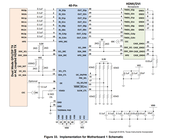
In the circuit implemented for DP++, the following point confuses me: the MOS transistor has a body diode. Because of this body diode, it appears that AUXP and AUXN can conduct to the sink terminal at any time.Does this circuit truly enable the self-identification function between AUX and DDC?

  • Hi,

    The diagram is not correct and we fixed it in our e2e FAQ.

    The AUXP has 100k pulled to GND, and the 100k to GND is placed between the MOSFET and receptacle. 

    The AUXN has 100k pulled to DP_PWR, and the 100k to DP_PWR is placed between the MOSFET and receptacle. 

    The source is a DP++ source with the DDC and AUX MUXED together as shown below.

    The CAD signal is connected to CFG1 of the receptacle and will also have a 1M weak pulldown to GND.

    Typically a DP sink will have its CFG1 floating, so when a DP sink connected, the CAD will be low due to the 1M weak pulldown. The MOSFET will then be open so you will have the 100nF plus the 100k pullup/pulldown for the normal AUX traffic.

    When a HDMI adaptor is connected, it will have a 100k pullup on CFG1, so CAD will be high and the MOSFET will short across the 100nF capacitor. The HDMI adaptor typically will have a 2k or a 4.7k pullup resistor on both AUXP/AUXN which will over-drive the 100k pullup/pulldown 

    Thanks

    David

  • thanks for reply. I understand what you're saying, but what confuses me is that when the CAD signal is low, the MOSFET is turned off. However, due to the MOSFET's body diode, the AUXP/N at the source side flows to the receptacle side through the MOSFET's body diode,right?

  • Hi,

    You are correct, and we need to modify the block diagram again. 

    You would need another MOSFET placed in opposite direction, drain to source, to block the flow through the body diode.

    CONFG1 to CAD would also require two MOSFET.

    We will update the block diagram and provide it to you.

    Thanks

    David

  • Many thanks, waiting for your new block diagram.

  • Hi,

    Please see updated block diagram.

    Thanks

    David

  • Got it.

    There's one more thing that has me really confused. The DP differential pair signals are AC-coupled, but HDMI's TMDS is DC-coupled. If I'm not mistaken, converting DP to HDMI requires an AC-coupling combined with a level-shifting circuit that includes a 499-ohm resistor to ground. However, in the DP++ circuit, I only see AC-coupling capacitors. So, from a hardware perspective, how does DP++ meet the transmission requirements for both DP and HDMI signals? Does the passive DP-to-HDMI adapter already include a circuit with a 499-ohm resistor to ground?