Part Number: DS125DF1610
Other Parts Discussed in Thread: DS250DF410
Tool/software:
Hi Team,
One of our customers is currently evaluating a circuit design that incorporates your product DS125DF1610 to generate PRBS signals.
To support this evaluation, we have purchased your EVM board and performed some initial validation using the GUI tool provided by your company. So far, the results have met our expectations.
However, both we and our customer have some specific application-related questions that we would like to clarify.
Thank you in advance for your assistance.
Our questions are as follows:
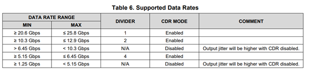
- With an RX input of 550 MHz, is it possible for the TX output to reach 5.5 GHz (550 MHz × 10) or 11 GHz (550 MHz × 20)? Is there a limitation that the TX frequency must be within 8× of the RX frequency?
- If we use the DS250DF410 (supports up to 25 Gbps with x2 and x4 sub-rate) to design an external 20 Gbps source, does the ATE need to provide at least a 5 Gbps signal (20/4) to the retimer RX?
- If the retimer can invert PRBS data, is it possible to control PRBS inversion via register settings?
Ex.
Normal PRBS7: 1000000100000110000101000111100100010110011101010011111010000111000100100110110101101111011000110100101110111001100101010111111
Inverted PRBS7: 0111111011111001111010111000011011101001100010101100000101111000111011011001001010010000100111001011010001000110011010101000000
- We noticed that this device supports JTAG Boundary Scan testing and that a BSDL (Boundary Scan Description Language) file is available in the DS125DF1610 programming guide.
Could you also provide a STIL (Standard Test Interface Language) file?
- Currently, we are using the TI GUI tool to control the device. We would like to transition to controlling the DS125DF1610 directly via SMBus using ATE I/O channels.
Could you kindly provide guidance or direct us to the appropriate contact for this?
We appreciate your support and look forward to your response.
Regards,
Neil Hung
Regards,
Neil