This thread has been locked.

If you have a related question, please click the "Ask a related question" button in the top right corner. The newly created question will be automatically linked to this question.

DS90UB926Q-Q1: FPD LINK III

Part Number: DS90UB926Q-Q1
Other Parts Discussed in Thread: DS90UB928Q-Q1, DS90UB947-Q1, DS90UB981-Q1

Tool/software:

Background:
A Qualcomm 8295 platform car product requires the use of TI's FPD LINK chip.


Question:
We want to use the DS90UB928Q-Q1  to use FPD LINK III. However, the current screen resolution of 480 * 480 is not sufficient to meet the requirement of PCLK>25M for FPD LINK III.

If the resolution is increased to a resolution of 584 * 720, it can meet PCLK>25M, but the estimated MIPI rate exceeds 500Mbps and does not meet the requirements of the display module.


I would like to ask if there is any solution to solve this problem.

  • Hello,

    Do you have a block diagram of the video path (serializer, deserializer, TCON/display) so I can make sure everything is clear? 

    If the resolution is increased to a resolution of 584 * 720, it can meet PCLK>25M, but the estimated MIPI rate exceeds 500Mbps and does not meet the requirements of the display module.

    How are you calculating that a MIPI rate of 500Mbps would be exceeded with a PCLK around 25MHz? For a PCLK of 25MHz, a DSI rate can be calculated by (PCLK * 12 / Number of Lanes) * 2. How many MIPI lanes are used?

    Best,

    Jack

  • Hi Jack,

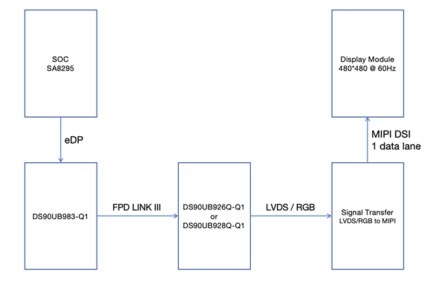
    The block diagram is as shown:

    I have to transfer a 584*720 resolution image to ensure that PCLK > 25M.

    The display module support only 1 data lane, so the DSI rata for 584*720 resolution would be 600Mbps (25MHz * 12 / 1 * 2) which could not meet the requirement of the display module.

    Is there a way to use FPD LINK III while keeping the DSI rate below 500Mbps?

  • Hi Tengfei,

    The minimum PCLK supported by the 983 in FPD-Link III mode is 25MHz. This is the only DP serializer so if the serializer cannot be changed then I do not see a solution beyond seeing if there is a display module that can support more than one DSI lane.

    If the serializer could be changed, a potential solution would be using a DP to LVDS converter IC (non-TI part) and using a DS90UB927-Q1 as the serializer. 

    Best,

    Jack

  • Hi Jack,

    Based on the current situation, I can only use FPD LINK IV, right?

    So, what are the deserializer chips that can be paired with it?

  • Hi Tengfei,

    Minimum PCLK supported with FPD-Link IV mode is 8MHz so this is a possible solution. The DS90UB988-Q1 is an FPD-Link IV OLDI deserializer. The other FPD-Link IV deserializer is the DS90UB984-Q1 which supports eDP.

    Best,

    Jack

  • Hi Jack,

    What is the reason for FPD LINK III's requirement for PCLK > 25M? Does this requirement apply to all serializers that support FPD LINK III?

    If not all FPD LINK III serializers require PCLK>25M, which serializers would have this requirement?

    Thanks!

  • ADD

    If 983 is used as the DP serializer and DS90UB926-Q1 is used as the deserializer (PCLK ≥ 25MHz), can 926 output RGB565 format data?
    Are there any requirements for the DP signal of SOC or the configuration of 983? Or is it sufficient to only configure 926 as the output format of RGB565?

  • Hi Tengfei,

    What is the reason for FPD LINK III's requirement for PCLK > 25M? Does this requirement apply to all serializers that support FPD LINK III?

    If not all FPD LINK III serializers require PCLK>25M, which serializers would have this requirement?

    For devices that support FPD-Link III operation, the minimum PCLK is not set to 25MHz for all devices. FPD-Link III devices such as the DS90UB925-Q1 and the DS90UB927-Q1 support PCLK operation down to 5MHz. Not all FPD-Link III devices support 5MHz minimum PCLK such as the DS90UB947-Q1.

    As the devices begin to support higher PLL rates it becomes difficult to keep the minimum PLL rate at the same rate as before. 

    If 983 is used as the DP serializer and DS90UB926-Q1 is used as the deserializer (PCLK ≥ 25MHz), can 926 output RGB565 format data?


    18-bit RGB and 24-bit RGB are the natively supported video data formats for FPD-Link III mode. If the TCON can only support RGB565, the unused lines from the 926 can be left as no connect.

    Best,

    Jack

  • Hi Jack,

    Does the DS90UB981-Q1 serializer also require PCLK>25MHz if FPD LINK III is to be used?

  • Hi Tengfei,

    The UB981 also requires a PCLK > 25MHz if operating in FPD-Link III mode.

    Best,

    Jack

  • Hi Jack,

    Thank you for your patience.

    I have a question regarding FPD-Link III wiring. The plan is to use a shielded twisted-pair cable, and a 24-pin USB Type-C connector will be used as an adapter in the middle. How can we evaluate whether such a wiring harness meets the signal requirements for FPD-Link III?

    The connection diagram is shown below.

    Thanks.

  • Hi Tengfei,

    The channel specifications for FPD-Link devices is only available under NDA only so I cannot release them on this forum. Do you have a local TI representative you can reach out for setting up an NDA?

    Best,

    Jack

  • Hi Jack,

    Please advise what specific documents I need to apply for the cable evaluation, and I can contact the local TI office to apply for them.

    Additionally, can the DS90UB926 process the deserialized image? For example, if the image resolution transmitted via FPD-Link III is 584×720@60Hz (a tentative value that could be adjusted), is the DS90UB96 capable of outputting an image at 480×480@60Hz?

  • Hi Tengfei,

    You will need to request the FPD-Link III channel specifications document. 

    The UB926 cannot resize the incoming video or adjust the bandwidth of the incoming video.

    Best,

    Jack

  • Hi Jack,

    When the serializer uses the 983 and communicates via FPD-Link III, could the 926 support the following timing output?

    Data foramt is R<7:0>G<7:0>B<7:0>.

    Are there any special requirements for the input from the 983?

    Thanks.

  • Hi Tengfei,

    I translated the horizontal video timing intervals into pixels for convenience

    Htotal = 718 pixels

    Hactive = 480

    Hsync = 20

    HBP = 28

    HFP = 190

    The 983 has the following constrains for horizontal video timing

    • HBP, Hsync, and Htotal must be divisible by 4
    • Horizontal blanking time is recommended to be >100 pixels
    • Hsync must be greater than 12 pixels

    With the current horizontal video timing, the following needs to be adjusted

    • Htotal needs divisible by 4

    Beyond the Htotal needing to be dividisible by 4, the 983 and 926 can support this video timing.

    Do you only have the nominal video time intervals for the display? Are the min/max intervals known?

    Best,

    Jack

  • Hi Jack,

    What do "min/max intervals" specifically refer to? I don't quite understand.

    Thanks.

  • Hi Tengfei,

    Most displays specify a minimum and maximum for video timings. Does the display in this system list the timing parameters with any tolerances? I've pasted an example below.

  • Hi Jack,

    I adjusted the timing parameters, please check if there are any issues now. And the RGB signals from 926 would be transmitted to a MIPI conversion chip, not directly to the display module, so there are no minimum and maximum for video timings.

    How is timing converted into pixels? Could you provide the calculation method?

    Thanks!

  • Hi Tengfei,

    Timing is converted into pixels by using the PCLK and multiplying the horizontal timing parameters by the PCLK. The PCLK units can be thought of as pixels per second.

    HPW = 800ns * 25MHz = 20 pixels

    HBP = 28 pixels

    HDP = 480 pixels

    HFP = 188 pixels

    HT = 716 pixels

    Timing parameters look good. No further comments on my end.

    Best,

    Jack

  • Hi Jack,

    please help rreview the schematic design.

    Thanks!

  • Hi Jack,

    Since our equipment only has the 926 (deserializer), during production testing, we would need a serializer to provide the FPD-Link III signal to the 926. The serializers are installed on the PCBA designed by another supplier, and the quantity available to us is limited.

    Are there any solutions for this situation? Developing a production test fixture with the serializer would be too costly. I'm wondering if we can use the 983's demo board to complete the production testing? Or do you have any other suggestion?

    Thanks!

  • Hi Tengfei,

    I will provide feedback on the 926 schematic by Wednesday at the latest.

    Are there any solutions for this situation? Developing a production test fixture with the serializer would be too costly. I'm wondering if we can use the 983's demo board to complete the production testing? Or do you have any other suggestion?

    The 983 EVM can be used for evaluating the functional capabilities of the serializer. The 983 does not contain EDID so any DPTX used with the 983 must have the capability of forcing video timings. 

    Best,

    Jack

  • Hi Jack,

    I have four questions that I'd like to ask for your help:

    1. I don't quite understand what you mean by "any DPTX used with the 983 must have the capability of forcing video timings."

    2. I'd like to know what additional accessories are needed if we use the 983 EVM. For example, where does the image content that the 983 sends to the 926 come from? Could it be transmitted from a PC to the 983?

    3. I could not find the user guide for the 983 EVM on the TI website, could you provide it?

    4. When the DS90UB926 is powered with 3.3V on both VDD33 and VDDIO, and the PCLK is 25MHz (using the timing discussed previously), what is the current consumption of VDD33 and VDDIO under operating conditions?

    Thanks!

  • Hi Tengfei,

    1. I don't quite understand what you mean by "any DPTX used with the 983 must have the capability of forcing video timings."

    The DPTX (laptop, SoC, etc.) cannot rely on reading EDID from the 983 to determine the resolution and video timings. The 983 does not support EDID so the DPTX needs to be programmed with the correct video timing.

    2. I'd like to know what additional accessories are needed if we use the 983 EVM. For example, where does the image content that the 983 sends to the 926 come from? Could it be transmitted from a PC to the 983?

    Yes, a PC can be used as the DPTX. A PC with a graphics card such as an Nvidia Quadro must be used since it will provide the ability to force EDID. Most consumer DPTX sources do not allow for forcing video timings so this needs to be considered.

    3. I could not find the user guide for the 983 EVM on the TI website, could you provide it?

    The collateral for the 983 is only available under NDA only. If you do not have a local TI contact, I can reach out to you over email in order to setup the NDA to access collateral for the 983.

    4. When the DS90UB926 is powered with 3.3V on both VDD33 and VDDIO, and the PCLK is 25MHz (using the timing discussed previously), what is the current consumption of VDD33 and VDDIO under operating conditions?

    You can refer to the previous E2E about UB926 power consumption.

    https://e2e.ti.com/support/interface-group/interface---internal/f/interface---internal-forum/1094879/ds90ub926q-q1-question-about-calculating-power-consumption-with-lower-pclk-frequency?tisearch=e2e-sitesearch&keymatch=ds90u%25252525252A926%252525252520AND%252525252520power#

    Best,

    Jack

  • Hi Tengfei,

    Below is my feedback on the UB926 schematic

    • Tie RES0 and RES1 to GND
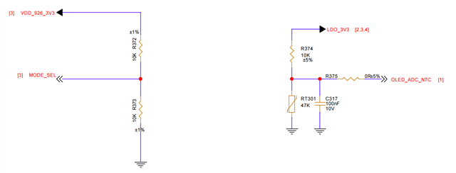
    • What MODE_SEL number are you targeting?
      • Based on your requirements, should be Mode No. 1 (LFMODE = L, Repeater  = L, Backward Compatible = L, I2S = L)
    • For FPD-Link AC coupling caps and CMF cap, the recommended voltage rating is 50v. Using 16v rating is fine if the expected DC level on the cable is to not exceed 1/4 of the voltage rating
    • Set BISTEN low to prevent the UB926 entering BIST (Built In Self Test) mode at startup
    • What IDx mode are you setting?
      • Most users tie IDx low to choose 0x58 as UB926 I2C address
    • Route FPD-Link traces as 100Ω differential
    • Are there pull-ups on the SDA and SCL lines on another schematic?
    • It is recommended to add 0.1µF decoupling caps for all power pins. The 0.1µF decoupling caps are recommended to be placed as close to the power pin as possible

    Best,

    Jack

  • Hi Jack,

    1.Could we implement the Production Line Testing with some other serializer or method? I thing that our primary goal is to ensure that the signal path—from the FPD-Link signal connector input to the output of the 926—is functioning correctly in the Production Line Testing. Given this objective, are there alternative serializer modules that are simpler to operate that we could use? Alternatively, could we employ a method such as sourcing an image from a computer's USB 2.0 port and then converting it into an FPD-Link III signal that matches our timing requirements?

    2.The link page about UB926 power consumption is unavailable, the page no longer exists. Could you give me the key words to search?

    Thanks!

  • Hi Jack,

    The FPD-Link III signal is connected to our mainboard via an STP cable. It then needs to be transmitted from the mainboard to another PCB through a micro coaxial cable. Could you please confirm if this connection is acceptable? Also, does the micro coaxial cable from the mainboard to another PCB need to meet a single-ended 50-ohm impedance requirement?

  • Hi Jack,

    what's the mismatch tolerance of length match on R, G, B, HS, VS,DE, PCLK traces?

    Thanks!

  • Hi Tengfei,

    1.Could we implement the Production Line Testing with some other serializer or method? I thing that our primary goal is to ensure that the signal path—from the FPD-Link signal connector input to the output of the 926—is functioning correctly in the Production Line Testing. Given this objective, are there alternative serializer modules that are simpler to operate that we could use? Alternatively, could we employ a method such as sourcing an image from a computer's USB 2.0 port and then converting it into an FPD-Link III signal that matches our timing requirements?

    You could still use the 983 for this purpose but instead of using the DP input the 983's internal pattern generator can send an image instead. Other serializers such as the UB949 could support internal PATGEN and video from a laptop.

    2.The link page about UB926 power consumption is unavailable, the page no longer exists. Could you give me the key words to search?

    The link I sent is to a forum which is restricted. I'll paste the contents below.

    We do not have any power over PCLK data for this part, but I can say that PCLK rate is not a major contributor to the power consumption of the device. 

    You can get a feel by looking at the table from the datasheet:

    In that data you can see that the difference between 85MHz and no video data (Without Input Stream) is only ~30mA on the core rail. So 26MHz is going to be somewhere between those two numbers. The bulk of the power comes from fixed blocks that are always running at the same rate regardless of operating PCLK rate and digital leakage. 

    The FPD-Link III signal is connected to our mainboard via an STP cable. It then needs to be transmitted from the mainboard to another PCB through a micro coaxial cable. Could you please confirm if this connection is acceptable? Also, does the micro coaxial cable from the mainboard to another PCB need to meet a single-ended 50-ohm impedance requirement?

    What interconnect is allowing for the signal to go from coax to STP? Is there a PCB in-between that interfaces with the coax and STP cable? And is this planned for real production or just for testing?

    For a PCLK of 25MHz, you should still be able to get lock but I cannot confirm.

    what's the mismatch tolerance of length match on R, G, B, HS, VS,DE, PCLK traces?

    This will be specified by the RGB receiver. 

    Best,

    Jack

  • Hi Jack,

    1.You could still use the 983 for this purpose but instead of using the DP input the 983's internal pattern generator can send an image instead. Other serializers such as the UB949 could support internal PATGEN and video from a laptop.

    ——Do you mean we do not need PC to supply the DPTX? What resolution could the 983's internal pattern generator support( for example about 584*720) ? And what would be the content of image? Do you have sample image?

    2.  What interconnect is allowing for the signal to go from coax to STP? Is there a PCB in-between that interfaces with the coax and STP cable? And is this planned for real production or just for testing?

    ——The FPD LINK III signal would be transmitted from 983 through STP to our PCB first and traced to a LVDS connector on the PCB, the FPD LINK III signal would be transmitted through a coax to another sub PCB, and then trace to 926 on the sub PCB. This solution is planned for real production.

    3.New question: Since the 926 and the MCU are not on the same PCB, and constrained by the limited number of signal interfaces, the MCU cannot directly detect the LOCK signal from the 926. How can the MCU recognize the handshake status between the 983 and the 926? Could the SOC controlling the 983 complete the handshake recognition by detecting the LOCK signal state of the 983, and then transmit the handshake completion information via I2C over FPD-Link III to the 926, which then forwards it to the MCU through the 926's I2C interface? This is necessary because the screen must be powered on and initialized only after the handshake is completed.

    Thanks! 

  • Hi Tengfei,

    ——Do you mean we do not need PC to supply the DPTX? What resolution could the 983's internal pattern generator support( for example about 584*720) ? And what would be the content of image? Do you have sample image?

    The 983 PATGEN can support the following patterns shown below. Please note that there is a minimum horizontal active requirement of 1024 pixels for color bar or horizontally scaled patterns when using 24bpp. FPD3 devices such as the UB949 do not have this limitation for color bar PATGEN.

    ——The FPD LINK III signal would be transmitted from 983 through STP to our PCB first and traced to a LVDS connector on the PCB, the FPD LINK III signal would be transmitted through a coax to another sub PCB, and then trace to 926 on the sub PCB. This solution is planned for real production.

    Are you planning to measure the insertion loss and return loss of the FPD-Link channel?

    3.New question: Since the 926 and the MCU are not on the same PCB, and constrained by the limited number of signal interfaces, the MCU cannot directly detect the LOCK signal from the 926. How can the MCU recognize the handshake status between the 983 and the 926? Could the SOC controlling the 983 complete the handshake recognition by detecting the LOCK signal state of the 983, and then transmit the handshake completion information via I2C over FPD-Link III to the 926, which then forwards it to the MCU through the 926's I2C interface? This is necessary because the screen must be powered on and initialized only after the handshake is completed.

    There is not a "handshake" mechanism to establish lock between the 983 and 926. The 926 will lock onto the incoming FPD-Link signal provided by cycling through EQ settings until it can recover the embedded clock. The back-channel between the 926 and 983 contains the forward channel lock status so the 983 will know if it has locked to the 926. The 983 can use this signal to move forward with enabling the display.

    Best,

    Jack

  • Hi Jack,

    1. 983 PATGEN

    ——So the pattern resolution would be H: 1024 V:580?

    2.Are you planning to measure the insertion loss and return loss of the FPD-Link channel

    ——We could not measure the IL and RL, we think the risk is low since the rate of FPD LINK III would be about 600Mbps, and the frequency is about 300MHz.

    3.There is not a "handshake" mechanism to establish lock between the 983 and 926. 

    ——You mean the SOC could know the lock status of 983 and 926, and could transmit the lock status through I2C via FPD LINK III, and then the lock status could be transmitted to MCU through the I2C interface of 926, right?

    Thanks!

  • Hi Tengfei,

    ——So the pattern resolution would be H: 1024 V:580?

    The display in your system wouldn't be able to display properly with 1024 Hactive. The 983 PATGEN can output with lower Hactive but it cannot be the colors bars or horizontally scaled patterns. You could still do the solid color patterns and the vertically scaled patterns.

    ——You mean the SOC could know the lock status of 983 and 926, and could transmit the lock status through I2C via FPD LINK III, and then the lock status could be transmitted to MCU through the I2C interface of 926, right?

    The lock status of the 926 can be read in the 983 by checking the RX_LOCK_DET bit. In the 926, the lock status can be read through 926 register 0x1C[0].

    Best,

    Jack

  • Hi Jack,

    The display in your system wouldn't be able to display properly with 1024 Hactive. The 983 PATGEN can output with lower Hactive but it cannot be the colors bars or horizontally scaled patterns. You could still do the solid color patterns and the vertically scaled patterns.

    ——You mean that the 983 PATGEN could output about 584*720 resolution image or patterns? And I think the horizontally scaled patterns are quite similar to the vertical scaled patterns( It appears that only the display orientation of the image has been rotated by 90° ), would there be any impact on the verification testing?

    Thanks.

  • Hi Tengfei,

    The 983 PATGEN can output 584*720 resolution patterns. Examples of the vertically scaled black to blue and black to white patterns are shown below. Note that these patterns are done at 1920*1080 for this display in the photos below.

  • Hi Jack,

    Please help advise which model of the 983 demo board is suitable for our current requirements: we need to verify the generation and transmission of image patterns, as well as the functionality of sending DP from the PC side to the 983 for image display.

    Thanks!

  • Hi Tengfei,

    The 983 EVM is not publicly available and the PC for the DP source would require the ability to force video timings due to the 983 not supporting EDID. The other option would be to use the 949 EVM which can serialize HDMI input.

    If you are interested in the 983 EVM, I can reach out to you over email.

    Best,

    Jack

  • Hi Jack,

    I could contact the local sales representative. Is the 983 EVM only available for provision by contacting you?

    Additionally, regarding the PC requirements, is the main point that the graphics card needs to support forcing video timings?

    Could you tell me the suitable EVM models for 983 and 926 that match my current verification needs?

    My e-mail address:

    tengfei.li@tinno.com

    Thanks!

  • Hi Tengfei,

    Start out with contacting the local sales representative and they will route your request through the appropriate channels. 

    Best,

    Jack

  • Hi Jack,

    The local sales said that the technical support of serdes could only be through this forum, right?

    And could you tell me the suitable model of 983 and 926 EVM, to facilitate better communication with the local sales representatives.

    What's more, could 926's BIST mode support 584*720 resolution patterns( the solid color patterns and the vertically scaled patterns)?

    How to calculate the supported resolution of PATGEN (926 and 983)?

    Thanks!

  • Hi Tengfei,

    I'll follow up with you over email. I will close out this thread for now.

    Best,

    Jack

  • Hi Jack,

    I adjusted the timing parameters, please check if there are any issues. 

    And the resolution would be 516*804.

    Since the DPTX fot the 983 is output by the SoC, what timing requirements do I need to specify for the SoC? Are they the same as the ones mentioned above?

    Thanks!

  • Hi Tengfei,

    The SoC will need to be programmed for the same video timing as the display. I calculated the correct number of lines for the vertical timings. I did not calculate the expected HFP with a given time of 4530.37ns. For a HFP of 300 pixels, this should be 12µs.

    One quick note: Display timings are stated using the Horizontal *  Vertical format. Be careful using Vertical * Horizontal as this may confuse others.

    Best,

    Jack