Other Parts Discussed in Thread: DS25BR204,
Tool/software:
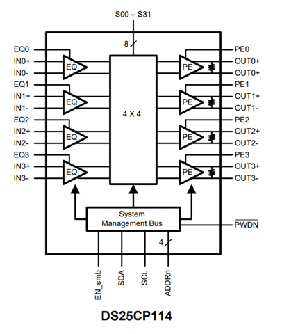
Hi TI team.
Could you please provide information on the IO state of the output pins when /PWDN=L?
Regards,
Matsumoto
Tool/software:
Hi TI team.
Could you please provide information on the IO state of the output pins when /PWDN=L?
Regards,
Matsumoto