Part Number: TCA9554
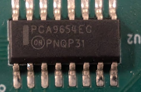
Other Parts Discussed in Thread: PCA9554
Tool/software:
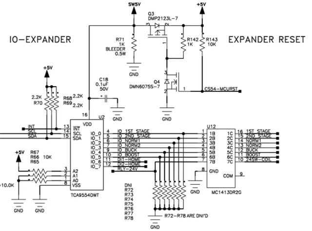
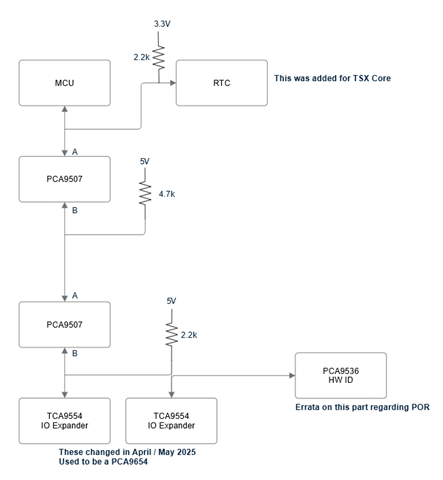
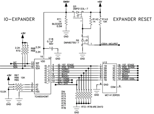
I have a system as shown above. There is a 6in harness in between the 9507s that route between two PCBs. We reset theTCA9554s with the following circuit:

As part of recovery and initial POR we bring the C554-MCURST signal active effectively removing power from the TCS9554
My questions are as follows:
1) If SCL or SDA is logic HIGH during the reset...is there any risk? Damage? Latch up? Improper reset?
2) If SCL and SDA are active (say communicating with the RTC in the block diagram why power is removed) during the reset...is there any risk? Damage? Latch up? Improper reset?
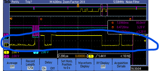
I'm experiencing an occasional lock/latch of this part when I write to it and the part issues and ACK; however, it did not process the written data. Then I subsequently read from it and it will only show all IOs as 0 (logic LOW) which matches the output pins. It's as if the write was ignored. I also do not think I have issues with proper HIGH / LOW voltage levels during the write.
Thanks,
-Rich