This thread has been locked.

If you have a related question, please click the "Ask a related question" button in the top right corner. The newly created question will be automatically linked to this question.

Custom PGA design using the TPL0102-100 Digital Potentiometer

Other Parts Discussed in Thread: TPL0102-100, OPA333

Dear all,

I am designing an  ultra low-power analog front-end for a sensor interface that will use a 12b ADC. In order to maximize the ADC DR, I need a PGA that will use an opa333 + a 2-channels digital potentiometer TPL0102-100 in the feedback path in a typical non-inverting amplifier configuration. I have 2 options:

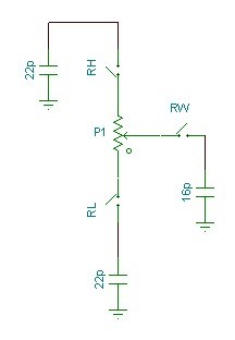
O1) Using 1 channel of the TPL0102-100 in Voltage Divider mode

O2) Using 2 channels of the TPL0102-100 in Rheostat mode

I have 4 questions:

A) Which option is best for gain accuracy? Being the gain dependent on Resistance ratios, is it better the ratio of Rhw/Rwl (O1) or rather R1/R2 (O2)? Is it correct stating that with O1 I should expect accuracy better than 0.5/256=2mV/V whereas for O2 it will be 2/256=7.8mV/V?

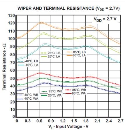
B) Which option is best for non linear distortion considering I will use a 3.3V supply with about 3Vpk-pk of output signal swing? In voltage mode I see 0.03% THD (for only 1Vrms) which would give max 70dB DR which means I would eat up part of my 12b ADC DR (ideally 74dB). Is that correct? How about the rheostat mode non linearity?

C) O1 will give me a worse case bandwidth of about BW=1/(2*pi*50kOhm*(10+16)pF)~122kHz  whereas O2 gives BW=1/(2*pi*100kOhm*(10+22)pF)~50kHz. Can you confirm that both options would be ok as far as BW having a 2kHz max signal frequency and sampling @ 8kHz?

D) Is there a PSPICE model available for the TPL0102-100 somewhere or what is the fastest way to test it around an opamp?

I look forward to hearing from you.

Best Regards,

Vito

  • Hi Vito,

    What ranges of gain are you looking to achieve w/ this PGA?

    A) The linearity values that we provide in our datasheet are "relative" linearity values (i.e. linearity after zero-scale and full-scale offset errors are removed).  Please take this into account if you're expecting a certain absolute accuracy since some error will be introduced once you get close in magnitude to the offset errors.  That being said, both configurations should give you very similar accuracies, but one drawback of the O1 configuration is that it will not allow you to adjust the gain in linear steps (ratio Rhw/Rwl is not linear).  The error introduced in O2 will simply be the error of a single channel in rheostat mode (other channel is constant).

    B) The main source of distortion in the dpot are the voltage dependencies of the Rh, Rl, and Rw switches.  If your output is swinging rail-to-rail, the switch that is connected to the output would definitely be the biggest concern.  It may be better to use a discrete resistor in the feedback path and/or switch to a differential topology to maximize your DR.  If neither of these options are possible, I would recommend using the entire 100k as your feedback resistor to minimize parasitic effects.  In particular, set that particular dpot channel to code 0x00h and tie terminals W and L together with both tied to the op-amp output (the RL and RW switches will be in parallel and hence the voltage dependency of these switches will be reduced).

    C) The dominant node of the O2 configuration will actually be the negative input terminal of the op-amp.  In this case, the worst case BW would be BW=1/(2*pi*R1||R2*Cp)=1/(2*pi*100k||100k*(22p+16p+4p))~75kHz.  I believe that this should be plenty of margin for your application.  Note that since this value is a bit smaller than the unity gain bandwidth of the op-amp, you will need to have a small capacitor across the feedback resistor in order to avoid any peaking in your frequency response (since the op-amp will become open-loop beyond the BW of your feedback network).

    D) Unfortunately we don't have any PSPICE models.  For AC simulations, please use the macromodel that has been provided in the datasheet.  For distortion simulations, please use voltage dependent resistors to model the dpot switches (CMOS switches vary ~30-40% across voltage).  We do have EVM kits available though and so if you're interested, please email akhil.nair@ti.com to request one.

    Best Regards,

    Jim

  • Dear Jim,

    thanks a lot for the detailed answer. 

    I am interested in a 2 to 11 gain range with the smallest gain step possible to eventually calibrate some gain error.

    Hereby my comments:

    A) Indeed I plan to calibrate both offset and gain error. A linear step is indeed convenient for an easier calibration.

    B) I wish I could use a differential topology: unfortunately I have a single-ended input and a single-ended ADC input (ADC12 in MSP430). I had in mind to do like you suggest for option O2 (also to be almost immune to the +/-20% tolerance), however I am still concerned that even 2 switches in parallel will give me some distortion with a 3Vpp voltage swing at the output, also considering I need -80dB THD. As I cannot simulate and test it (at the moment), could you please roughly quantify the distortion I should expect in such case?

    C) Good point, thank you.

    D) Could you please provide me with a more accurate macromodel than in the datasheet? More in detail, where/how are the CMOS switches placed exactly? Can you post a rough schematic drawing please? That would help as I can try to place most switches on the virtual ground where there should be barely signal.

    Thanks a lot again.

    Vito

  • Hi Vito,

    I tried taking a look at the distortion introduced when the dpots are used in feedback configuration with a couple sims and it looks like the effect of the switch resistance variation has very strong impact on the overall gain function and hence the distortion ends up being significantly magnified (compared to when the dpot is used as a voltage divider).  I don't think that this approach will be sufficient for your needs.

    Something else that you might try is using the amplifer as a fixed gain stage w/ discrete resistors and then using the dpot at the input of this gain stage as a voltage divider to attenuate the signal as necessary.  Your -80dB THD requirement will definitely still be a challenge, but I think that you may get very close.  The spec that we have on our datasheet is actually a THD+N measurement using a 80kHz bandwidth and so that number is a bit pessimistic if you're concerned w/ the distortion only.  To give you feel for the distortion levels to expect, my sims are showing that the THD alone is on the order of 0.005%.

    Finally, I've attached a figure showing you how the switches are connected to the dpot terminals and a plot of the switch resistance variation with voltage (plot from TPL0202 datasheet).

    Hope that helps.

    Best Regards,

    Jim