TIOS102: The leakage current in reverse polarity is high

Part Number: TIOS102


Hi,

We use the TIOS102 for the IO Link design, and now, we have below leakage current in reverse polarity issue;

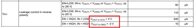
  1. We set the IN to 0V and set the EN to 3.3V, onnected the external power supply VCC-IN to the OUT pin through an ammeter. There is a description of reverse polarity protection in the specification sheet  why is there still a leakage current of around 18mA in actual testing? 
  2. The input voltage is 19-28.8V, and the output current is 250mA;
  3. The normal leakage current is 640uA max. in the datasheet;
  4. Please refer to below schematic diagram and check if there are any error for our design;9146e085e72639b55f0a09eef54fada1.jpg
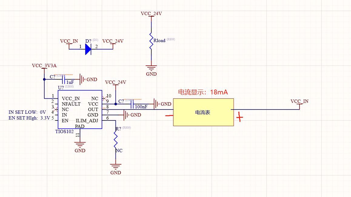
  5. We add the a diode to the VCC and the leakage current is about 540uA;bfbf17f5cf0d45eab44b178b625fa145.jpg
  • Hi Zhang,

    The Reverse Polarity Detection circuits in the device will engage when there is a voltage difference between the OUT, VCC and GND pins of approximately 100mV.  

    If the High Side Driver is active the OUT pin will be connected to the VCC pin through the driver transistors with a Rdson of approximately 2.5 ohms.  If the OUT pin voltage becomes greater than the VCC pin voltage by 100mV, the detection comparator will trip and the driver transistors will become disabled and enter a diode blocking mode where they block the flow of reverse current.

    In your current configuration you have an internal 2.5 ohm (Rdson) connection between the VCC and OUT pins internal to the device, and an external connection with a Diode placed between the VCC and OUT pins through the Ammeter.

    There needs to be enough current flow across the Rdson to create a 100mV difference between the VCC and OUT pins so that the driver becomes disabled.  Until then the driver transistors will function in a resistive mode and the VCC and OUT pins will be connected by the Rdson of the transistors.

    Likewise the Low Side driver has the same situation where the OUT pin needs to be less than the GND pin by 100mV to engage the Reverse Polarity Detection circuits.  If the Low Side Driver is enabled, the OUT pin will need to be pulled low enough such that there is at least a 100mV voltage drop across the 2.5 ohm Rdson of the driver transistors.  Otherwise the OUT and GND pins will be connected by a 2.5 ohm Rdson resistance.

    The datasheet specification you have referred to has a 640uA max specification when the OUT pin and VCC or GND pin voltage difference is 3V which is large enough to ensure the required voltage drop to disable the driver transistors and block any flow of current.

    Regards,

    Jonathan