A related question is a question created from another question. When the related question is created, it will be automatically linked to the original question.
If you have a related question, please click the "Ask a related question" button in the top right corner. The newly created question will be automatically linked to this question.
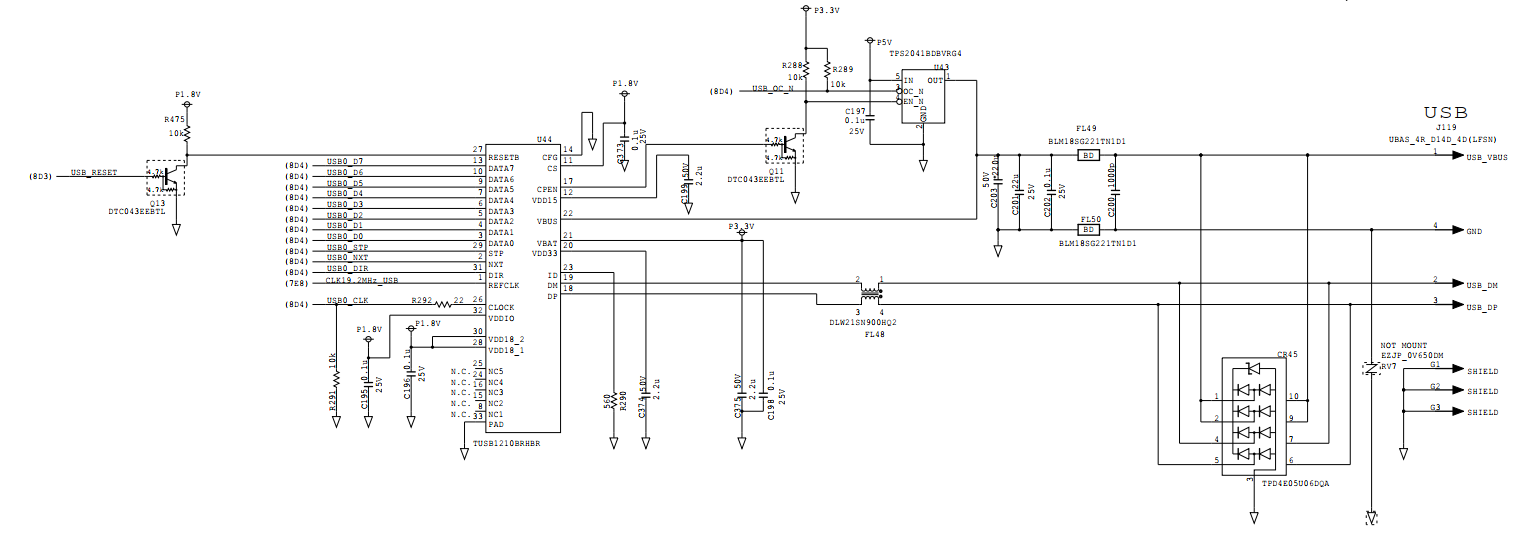
TUSB1210: Regarding Circuit Design Using TUSB1210BRHBR
Currently planning to use TUSB1210BRHBR for circuit design, with the device functioning as a USB host. The circuit diagram is shown below. Please help confirm if there are any design issues. Thank you.
1、The current target is a host application, and the TUSB1210BRHBR is operating in HOST mode.
2、Regarding your suggestion to add 22Ω resistors to all ULPI signal lines (DATA0–7, DIR, STP, NXT, CLOCK): since damping resistors are typically placed at the signal output end, should they be added to the output pins of these signals? Also, since DATA0–7 are bidirectional signals, how should the 22Ω resistors be applied?
Can I refer to the following diagram (SLLU208) for the 22Ω resistor configuration?Is it acceptable to place all the 22Ω resistors on the TUSB1210BRHBR side as shown in the diagram below? Do we still need to place 22Ω resistors on the SoC side that interfaces with it?
3、Regarding decoupling capacitors, your suggestion is that both VDD18_1 and VDD18_2 require independent decoupling capacitors. Is my understanding correct?
4、REFCLK is sourced from an external 3.3V crystal oscillator.
5、Regarding the ID signal, the datasheet recommends using a resistor less than 1kΩ. We are currently using a 560Ω resistor (0402 package) — is this acceptable?
Regarding the placement of the 22Ω damping resistors, I still have some questions and hope you can provide confirmation. Following the principle of placing damping resistors near the driving source:
STP signals are placed near the SOC pins.
NXT, DIR, and CLOCK are placed near the TUSB1210 pins.
However, how should the damping resistors for (DATA0-7) be placed? Should 22Ω resistors be placed on both the SOC and TUSB1210 sides? Please confirm. Thank you.
Additionally, does TI have any relevant technical documentation on this matter?