This thread has been locked.

If you have a related question, please click the "Ask a related question" button in the top right corner. The newly created question will be automatically linked to this question.

TLIN1028EVM: pull down resistor at TXD pin and how to improve BCI performance

Part Number: TLIN1028EVM

Hi team,

Please help to provide some comments for the questions below.

  1. In EVM shematic, there is a 51ohm pull down resistor at TXD pin, what's the function of it? Meanwhile, there is also a 350kohm internal pull up resistor, what's the benifit?image.png
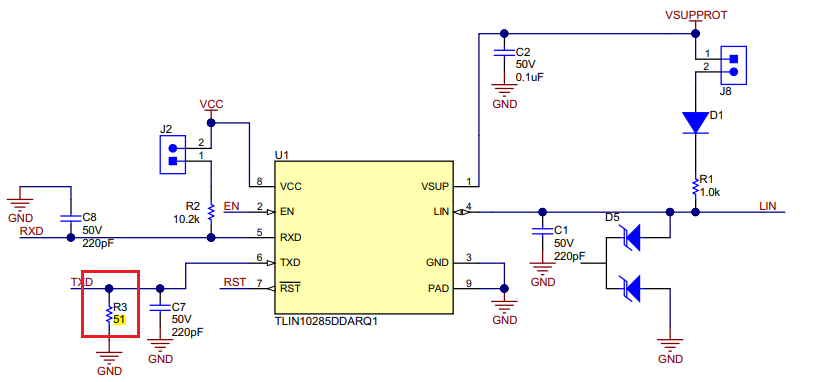
  2. For internal resitor at TXD pin, In TLIN1028 it is a pull-up resistor, while in other devices it is pull-down(like TLIN1039). What's the difference of them, if possible, is a pull-up or pull-down more advisable, why?
  3. When the customer conducted BCI testing in accordance with ISO11452-4-2020 standard, they found that the device failed to operate normally under the test condition of 200mA injection, affected by interference below 15MHz bandwidth—while competitors’ chips performed properly. Below is the schematic diagram of the VSUP pin. A 100pF pull-down capacitor is connected to the TXD, RXD, and LIN pins, but no pull-down resistor is added to the TXD pin. Are there any measures to improve this performance, and will the pull-down resistor help address the issue?image.png

Regards,

Eileen

  • Hi Eileen,

    1. The internal pull-up ensures LIN is recessive when TXD is floating or left open. The EVM resistor is just for PAD placement to give users the flexibility for additional variations.

    2. This is based on their DTO features mentioned in their data sheets. It depends if customers have a preference on how their MCU should behave when disconnected. I.e., can choose as needed as pull-up for recessive by default implies unintended bus activity when MCU is disconnected and pull-down for dominant by default if customer relies on the TXD low for specific DTO / wake behaviors.

    3. BCI failures are typically layout / decoupling and harness injection related. VBAT decoupling looks good for above 20 to 30 MHz. The 15 MHz is most likely from couples through TXD/RXD/LIN/GND structures and will presume the 100 pF are close to the IC pins and not on the harness side. Pull-down on TXD helps in some cases, giving a return path for induced current. Series dampening resistors should help the most (33 - 100 ohms typical, and can adjust accordingly), while ensuring a solid GND loop with all caps returning to the same GND as the IC. See this report for more information on the device's BCI testing, thanks.

    Best Regards,

    Michael.

  • Hi Michael,

    Please check the schematic and layout from customer. Is there anything need to improve for the BCI test?

    Below are the schematic of the VSUP pin, other parts of schematic, layout. It’s difficult for customer to send SCH and PCB files due to the confidentiality.

    Regards,

    Eileen

  • Hi Eileen,

    Yes, could you help confirm including the series dampening resistor recommendation (33 - 100 ohms typical, and can adjust accordingly), while ensuring a solid GND loop with all caps returning to the same GND as the IC did not help while also comparing to this report on the device's BCI testing?

    Best Regards,

    Michael.

  • Hi Michael,

    The series dampening resistor you mean is at all of TXD, RXD, LIN and GND these four pins? And apart from this point, is there anything else needs to be improved in their schematic and layout?

    Regards,

    Eileen

  • Hi Eileen,

    The series dampening resistor is for the IO pins TXD / RXD and nothing additional as I would recommend to confirm if issues are mitigated and by how much, thanks.

    Best Regards,

    Michael.