Part Number: SN65DSI83
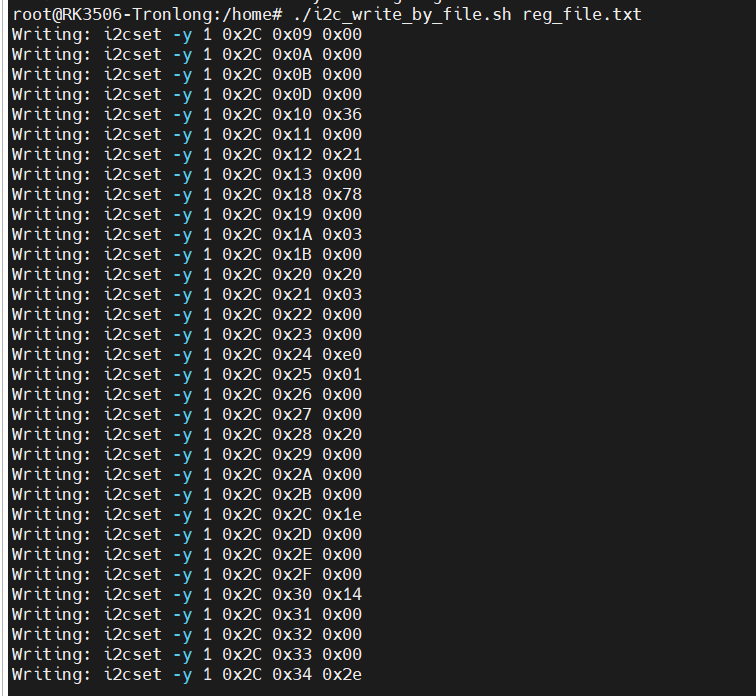
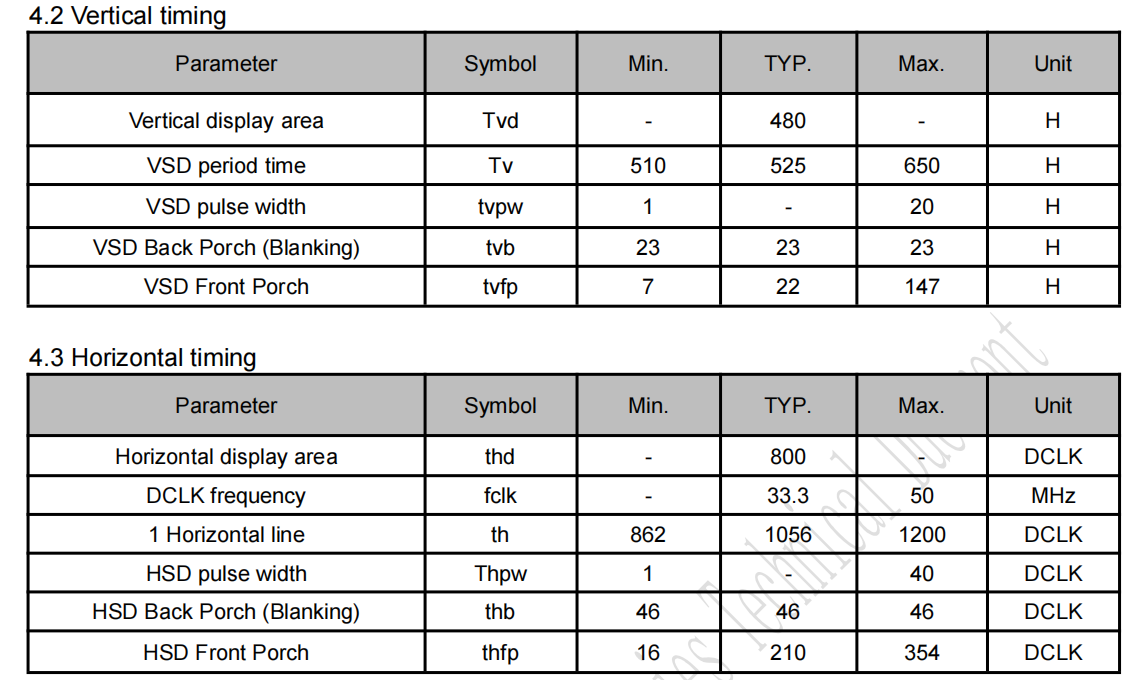
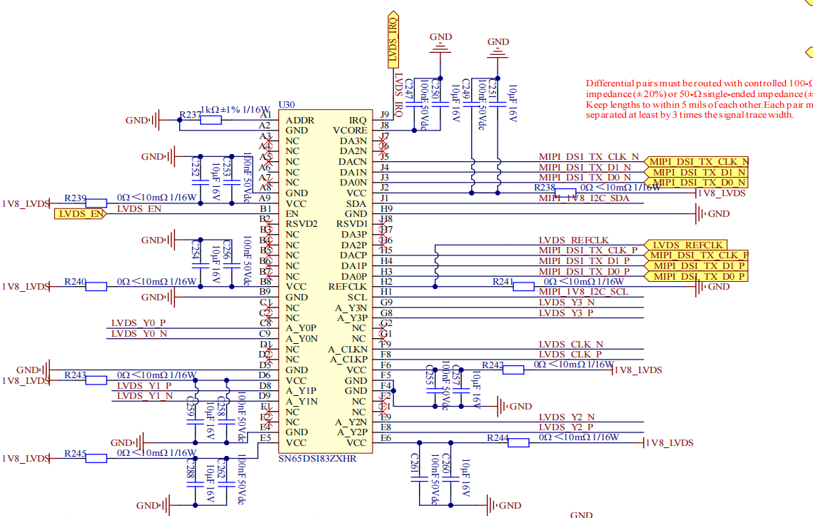
I am currently debugging MIPI to LVDS. First, I need to confirm whether the hardware is working properly. I can configure SN65DSI83 via I2C. I tried using the tunner tool to generate sequences, but the test pattern still doesn't display on the screen. It seems the clock is not aligned. I found a 24M clock that can be connected to the chip. May I ask how to configure the tunner? I have attached the schematic diagram and screen parameters.
Are there any precautions for controlling the enable pin of the chip?