DP83TC812S-Q1: RX data output abnormality

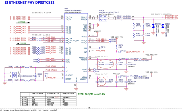
Part Number: DP83TC812S-Q1


Hi Teams,

The customer used DP83TC812SRHARQ1 and experienced abnormal RX data output.

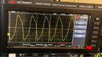
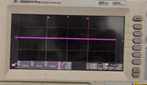
The 28PIN (J3_SGMII_TXCK) frequency of the PHY chip is 31MHz (stable output of 25MHz for good products), and there is no level change or network waveform for 29PIN. The measurement shows no level change or network waveform for pins 30-33 of the PHY chip (normal products have data waveform output). The measurement shows that the 15PIN-J3_SGMII_SXDV waveform has a normal frequency of 25MHz without any abnormalities, while the 27PIN-J3_SGMII-RXCK frequency is abnormal and jumps between 11.5M-25M (stable output of normal 25MHz), and there is no RX data output for pins 23-26M
Note: RGMII is an Ethernet data interface, RGMII-TXEN - send enable, RGMII-TXD0-D3- send data, RGMII-RXD0-D3- receive data
Summary: Abnormal TX/RX clock frequency of PHY chip leads to abnormal output network data of PHY chip.

image.png

image.pngimage.pngimage.pngimage.png

This issue has been reported to the FQE department, but their conclusion is to discuss it with the Application team. Please assist.

  • Hi Vayne,

    Pin 28 is an input clk from the MAC in RGMII.

    Does the XTAL meet the specified requirements?  Can you probe pin 16 (CLKOUT) to see a stable clock output from the PHY?

    Can you verify the pin-strap configuration, are there schematics that can be shared (How is the PHY being configured)?  

    Are all power supplies stable and within the correct levels?

    Is the RESET pin stable (Same level as VDDIO)?

    Regards,

    Undrea

  • Hi Undrea,

    The customer has answered the following question, please refer to it.

    1.Does the XTAL meet the specified requirements? Can you probe pin 16 (CLKOUT) to see a stable clock output from the PHY?
    A: Thet have actually measured the PHY crystal oscillator and found a stable output of 25MHz. However, they did not measure the 16PIN because in our actual circuit application, the 16PIN is an empty PIN
    2.Can you verify the pin-strap configuration, are there schematics that can be shared (How is the PHY being configured)?
    A: The following is the circuit schematic:

    3.Are all power supplies stable and within the correct levels?
    A: The power supply of PHY is completely consistent with the measured and good products, all within the specification range.

    4.Is the RESET pin stable (Same level as VDDIO)?
    A: The reset pin has a stable output of 1.8v, which is completely consistent with VDDIO.

    Thank you~

    BR

  • Hi Undrea,

    We look forward to your reply. The customer is quite anxious

  • Hi Undrea

    Could you please help check our answer?

    Customer is waiting for the answer, they have 5 pcs fail chips now. Thanks!

  • Closing. Please re-open if needed.