TDA4VL-Q1: SPI in/out test

Part Number: TDA4VL-Q1


Hi Ti,

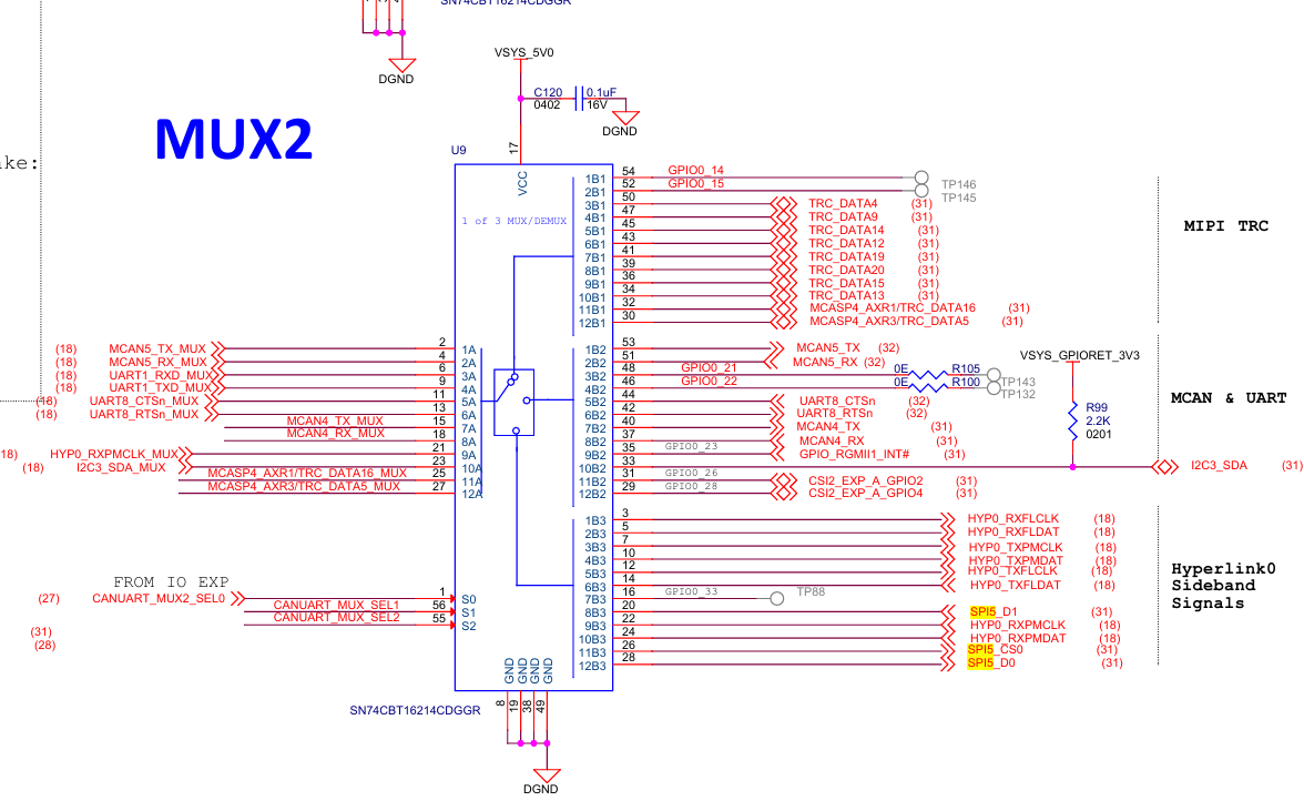
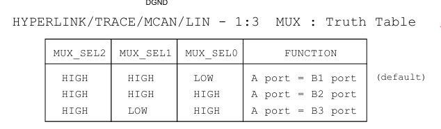
I want to test SPI external communication, so I'm using 'mcusw/mcal_drv/mcal/examples/Spi/mcspi_app/McspiApp.c' for testing. The circuit diagram shows that SPI5 needs to be used and 'CANUART_MUX' needs to be selected to port B3 for data transmission testing.

image.png

image.png

Therefore, I made the following modifications to 'McspiApp_Startup.c'. 

mcusw/mcal_drv/mcal/examples/Spi/mcspi_app/soc/j721s2/mcu2_1/McspiApp_Startup.c: McspiApp_Startup.c

Currently, it seems that whether D0 and D1 are shorted or not, the log shows that 'rx' successfully received the data transmitted by 'tx'.

I believe that shorting D0 and D1 will make the UART log show that 'rx' successfully received the data from 'tx'; without shorting, the UART log will show a mismatch or an inability to receive data.

image.png

Is there anything wrong with my testing method, modification method, or idea?

Thanks a lot!!

Alice

  • Hi Alice, 

    Thanks for your question, I directed it to one of our experts who will be getting back to you.

    Regards,
    Sarabesh S.

  • Hello Alice,

    If you short D0 and D1 you will receive the same data sent and acts as external loop back method.

    This MUX SEL0 port pin is hardware connected to switch as well please check the schematics.

    Which SDK version is this?

    Regards

    Tarun Mukesh 

  • Hi Tarun,

    If you short D0 and D1 you will receive the same data sent and acts as external loop back method.

    Currently, it seems that whether D0 and D1 are shorted or not, the log shows that 'rx' successfully received the data transmitted by 'tx'.

    I believe that shorting D0 and D1 will make the UART log show that 'rx' successfully received the data from 'tx'; without shorting, the UART log will show a mismatch or an inability to receive data.

    1. Because I can match rx and tx data with and without shorting, which is different from what I originally thought. Do you mean that shorting it results in an external loopback, and not shorting it results in an internal loopback? And do both external and internal loopbacks successfully transmit data?

    This MUX SEL0 port pin is hardware connected to switch as well please check the schematics.

    Therefore, I made the following modifications to 'McspiApp_Startup.c'. 

    mcusw/mcal_drv/mcal/examples/Spi/mcspi_app/soc/j721s2/mcu2_1/McspiApp_Startup.c: McspiApp_Startup.c

    2. I couldn't find a switch to connect to, so I added an IO expander setting in McspiApp_Startup.c.

    Which SDK version is this?

    3. ti-processor-sdk-rtos-j721s2-evm-10_01_00_04

    Thanks a lot,

    Alice

  • Hello Alice,

    First of all ,Happy new year.

    1. Because I can match rx and tx data with and without shorting, which is different from what I originally thought. Do you mean that shorting it results in an external loopback, and not shorting it results in an internal loopback? And do both external and internal loopbacks successfully transmit data?

    Let me give more detailed explanation,

    External Loop back:

    Consider D0 as Tranmission and D1 as Reception , D0 and D1 should be shorted so that you can get the same exact data send to received buffers.

    Internal Loop back:

    Consider D0 as Transmission and also as Reception then without any external shorting the D0 data sent will also be received into receive buffers.

    2. I couldn't find a switch to connect to, so I added an IO expander setting in McspiApp_Startup.c.

    Yes, sorry i checked for other device J784S4 . For J721S2 there is no switch 

    For example to control IO expander we will do as below in screen shot to drive. 

    This is only sample screen shot to drive IO expander not same should be used. 

     ti-processor-sdk-rtos-j721s2-evm-10_01_00_04

    Please consider taking latest SDK since 

    Latest SDK 11.0 and later versions have no issue in configuration whereas earlier version used to have some problems.

    https://sir.ext.ti.com/jira/browse/EXT_EP-12468

    Regards

    Tarun Mukesh

  • Hi Tarun,

    I want to test the external loopback, so I set D1 to RX and D0 to TX, with regval values ​​of 0x24000B and 0x00008 respectively.

    /*
    *
    * Copyright (c) 2024 Texas Instruments Incorporated
    *
    * All rights reserved not granted herein.
    *
    * Limited License.
    *
    * Texas Instruments Incorporated grants a world-wide, royalty-free, non-exclusive
    * license under copyrights and patents it now or hereafter owns or controls to make,
    * have made, use, import, offer to sell and sell ("Utilize") this software subject to the
    * terms herein.  With respect to the foregoing patent license, such license is granted
    * solely to the extent that any such patent is necessary to Utilize the software alone.
    * The patent license shall not apply to any combinations which include this software,
    * other than combinations with devices manufactured by or for TI ("TI Devices").
    * No hardware patent is licensed hereunder.
    *
    * Redistributions must preserve existing copyright notices and reproduce this license
    * (including the above copyright notice and the disclaimer and (if applicable) source
    * code license limitations below) in the documentation and/or other materials provided
    * with the distribution
    *
    * Redistribution and use in binary form, without modification, are permitted provided
    * that the following conditions are met:
    *
    * *       No reverse engineering, decompilation, or disassembly of this software is
    * permitted with respect to any software provided in binary form.
    *
    * *       any redistribution and use are licensed by TI for use only with TI Devices.
    *
    * *       Nothing shall obligate TI to provide you with source code for the software
    * licensed and provided to you in object code.
    *
    * If software source code is provided to you, modification and redistribution of the
    * source code are permitted provided that the following conditions are met:
    *
    * *       any redistribution and use of the source code, including any resulting derivative
    * works, are licensed by TI for use only with TI Devices.
    *
    * *       any redistribution and use of any object code compiled from the source code
    * and any resulting derivative works, are licensed by TI for use only with TI Devices.
    *
    * Neither the name of Texas Instruments Incorporated nor the names of its suppliers
    *
    * may be used to endorse or promote products derived from this software without
    * specific prior written permission.
    *
    * DISCLAIMER.
    *
    * THIS SOFTWARE IS PROVIDED BY TI AND TI'S LICENSORS "AS IS" AND ANY EXPRESS
    * OR IMPLIED WARRANTIES, INCLUDING, BUT NOT LIMITED TO, THE IMPLIED WARRANTIES
    * OF MERCHANTABILITY AND FITNESS FOR A PARTICULAR PURPOSE ARE DISCLAIMED.
    * IN NO EVENT SHALL TI AND TI'S LICENSORS BE LIABLE FOR ANY DIRECT, INDIRECT,
    * INCIDENTAL, SPECIAL, EXEMPLARY, OR CONSEQUENTIAL DAMAGES (INCLUDING,
    * BUT NOT LIMITED TO, PROCUREMENT OF SUBSTITUTE GOODS OR SERVICES; LOSS OF USE,
    * DATA, OR PROFITS; OR BUSINESS INTERRUPTION) HOWEVER CAUSED AND ON ANY THEORY
    * OF LIABILITY, WHETHER IN CONTRACT, STRICT LIABILITY, OR TORT (INCLUDING NEGLIGENCE
    * OR OTHERWISE) ARISING IN ANY WAY OUT OF THE USE OF THIS SOFTWARE, EVEN IF ADVISED
    * OF THE POSSIBILITY OF SUCH DAMAGE.
    *
    */
    
    /**
     *  \file     McspiApp_Startup.c
     *
     *  \brief    This file contains the pinmux, interrupt and clock configuration.
     */
    /* ========================================================================== */
    /*                             Include Files                                  */
    /* ========================================================================== */
    #include "McspiApp_Startup.h"
    #include "McspiApp.h"
    
    /* ========================================================================== */
    /*                         Structures and Enums                               */
    /* ========================================================================== */
    
    /* ========================================================================== */
    /*                 Internal Function Declarations                             */
    /* ========================================================================== */
    
    /* ========================================================================== */
    /*                            Global Variables                                */
    /* ========================================================================== */
    
    /* ========================================================================== */
    /*                          Function Definitions                              */
    /* ========================================================================== */
    /** \brief Start up sequence : Program the interrupt muxes / priorities */
    void SpiApp_Startup(void)
    {
        uint32 regVal;
    
        /* write Partition Lock Key 0 Register */
        CSL_REG32_WR(CSL_MCU_CTRL_MMR0_CFG0_BASE + CSL_MCU_CTRL_MMR_CFG0_LOCK1_KICK0,
            0x68EF3490U);
        /* write Partition Lock Key 1 Register */
        CSL_REG32_WR(CSL_MCU_CTRL_MMR0_CFG0_BASE + CSL_MCU_CTRL_MMR_CFG0_LOCK1_KICK1,
            0xD172BC5AU);
        /* Check for unlock */
        regVal = CSL_REG32_RD(CSL_MCU_CTRL_MMR0_CFG0_BASE + CSL_MCU_CTRL_MMR_CFG0_LOCK1_KICK0);
        while ((regVal & 0x1U) != 0x1U)
        {
            regVal = CSL_REG32_RD(CSL_MCU_CTRL_MMR0_CFG0_BASE + CSL_MCU_CTRL_MMR_CFG0_LOCK1_KICK0);
        }
    
        /* Unlock lock key registers for Partition 7: IO PAD
           configuration registers in MAIN_CTRL_MMR */
        /* write Partition 7 Lock Key 0 Register */
        CSL_REG32_WR(CSL_CTRL_MMR0_CFG0_BASE + CSL_MAIN_CTRL_MMR_CFG0_LOCK7_KICK0,
                    0x68EF3490);
        /* write Partition 7 Lock Key 1 Register */
        CSL_REG32_WR(CSL_CTRL_MMR0_CFG0_BASE + CSL_MAIN_CTRL_MMR_CFG0_LOCK7_KICK1,
                    0xD172BC5A);
        /* Check for unlock */
        regVal = CSL_REG32_RD(CSL_CTRL_MMR0_CFG0_BASE +
            CSL_MAIN_CTRL_MMR_CFG0_LOCK7_KICK0);
        while ((regVal & 0x1) != 0x1U)
        {
    		regVal = CSL_REG32_RD(CSL_CTRL_MMR0_CFG0_BASE +
                CSL_MAIN_CTRL_MMR_CFG0_LOCK7_KICK0);
        }
    
        /* Enable MCU_MCSPI1 and MCSPI3 independently pin out */
        CSL_REG32_WR(CSL_MCU_CTRL_MMR0_CFG0_BASE +
            CSL_MCU_CTRL_MMR_CFG0_MCU_SPI1_CTRL,
                CSL_MCU_CTRL_MMR_CFG0_MCU_SPI1_CTRL_SPI1_LINKDIS_MASK);
    
        /* MCSPI 5 CS0 PAD configuration */
        regVal = CSL_REG32_RD(CSL_CTRL_MMR0_CFG0_BASE + CSL_MAIN_CTRL_MMR_CFG0_PADCONFIG26);
        regVal = 0x40008U;
        CSL_REG32_WR(CSL_CTRL_MMR0_CFG0_BASE + CSL_MAIN_CTRL_MMR_CFG0_PADCONFIG26, regVal);
    
        /* MCSPI 5 CS1 PAD configuration */
        regVal = CSL_REG32_RD(CSL_CTRL_MMR0_CFG0_BASE + CSL_MAIN_CTRL_MMR_CFG0_PADCONFIG25);
        regVal = 0x40008U;
        CSL_REG32_WR(CSL_CTRL_MMR0_CFG0_BASE + CSL_MAIN_CTRL_MMR_CFG0_PADCONFIG25, regVal);
    
        /* MCSPI 5 CS2 PAD configuration */
        regVal = CSL_REG32_RD(CSL_CTRL_MMR0_CFG0_BASE + CSL_MAIN_CTRL_MMR_CFG0_PADCONFIG21);
        regVal = 0x40008U;
        CSL_REG32_WR(CSL_CTRL_MMR0_CFG0_BASE + CSL_MAIN_CTRL_MMR_CFG0_PADCONFIG21, regVal);
    
        /* MCSPI 5 CS3 PAD configuration */
        regVal = CSL_REG32_RD(CSL_CTRL_MMR0_CFG0_BASE + CSL_MAIN_CTRL_MMR_CFG0_PADCONFIG22);
        regVal = 0x40008U;
        CSL_REG32_WR(CSL_CTRL_MMR0_CFG0_BASE + CSL_MAIN_CTRL_MMR_CFG0_PADCONFIG22, regVal);
    
        /* MCSPI 5 D1 PAD configuration */
        regVal = CSL_REG32_RD(CSL_CTRL_MMR0_CFG0_BASE + CSL_MAIN_CTRL_MMR_CFG0_PADCONFIG34);
        regVal = 0x24000BU;
        CSL_REG32_WR(CSL_CTRL_MMR0_CFG0_BASE + CSL_MAIN_CTRL_MMR_CFG0_PADCONFIG34, regVal);
    
        /* MCSPI 5 D0 PAD configuration */
        regVal = CSL_REG32_RD(CSL_CTRL_MMR0_CFG0_BASE + CSL_MAIN_CTRL_MMR_CFG0_PADCONFIG28);
        regVal = 0x00008U;
        CSL_REG32_WR(CSL_CTRL_MMR0_CFG0_BASE + CSL_MAIN_CTRL_MMR_CFG0_PADCONFIG28, regVal);
    
        /* MCSPI 5 CLK PAD configuration */
        regVal = CSL_REG32_RD(CSL_CTRL_MMR0_CFG0_BASE + CSL_MAIN_CTRL_MMR_CFG0_PADCONFIG31);
        regVal = 0x40008U;
        CSL_REG32_WR(CSL_CTRL_MMR0_CFG0_BASE + CSL_MAIN_CTRL_MMR_CFG0_PADCONFIG31, regVal);
    
        setI2C();
        /* Initialize profiling API's */
        AppUtils_ProfileInit (0U);
    
        /* Initialize memory sections  */
    	AppUtils_SpiSectionInit();
    
        /* Interrup Registrations */
        SpiApp_InterruptConfig();
    
        return;
    }
    
    void setI2C(void)
    {
        uint32 regVal = 0U;
    
        I2C_Params      i2cParams;
        I2C_Handle      handle = NULL;
        uint8           dataToSlave[4];
    
        /*
         * Configuring TCA6408A IO Exp  with addr 0x21
         * This io expander is controlled by i2c0
         * For Main MCAN4 P07 should be set to 0.
         */
         /* I2c PinMux */
        /* I2C0_SDL */
        regVal = 0x40000U;
        CSL_REG32_WR(CSL_CTRL_MMR0_CFG0_BASE + 0x1C0E0U, regVal);
        /* I2C0_SDA */
        regVal = 0x40000U;
        CSL_REG32_WR(CSL_CTRL_MMR0_CFG0_BASE + 0x1C0E4U, regVal);
        /* I2C initialization */
        I2C_init();
        I2C_Params_init(&i2cParams);
        i2cParams.transferMode = I2C_MODE_BLOCKING;
        i2cParams.bitRate = I2C_400kHz;
        i2cParams.transferCallbackFxn = NULL;
    
        handle = I2C_open(0U, &i2cParams);
    
        /* ------------------- step 1 Read & write Configuration register ------------------------------------*/
        /* Read the Config port 0 */
        dataToSlave[0] = TCA6408A_REG_CONFIG0;
        dataToSlave[1] = 0x0U;
        SetupI2CTransfer(handle, 0x21, &dataToSlave[0], 1, &dataToSlave[1], 1);
        
        /* writing 0 to p07 , 0 -> output mode, 1 -> Input mode*/
        dataToSlave[0] = TCA6408A_REG_CONFIG0;
        dataToSlave[1] &= ~(1 << 1);
        dataToSlave[1] &= ~(1 << 2);
        dataToSlave[1] &= ~(1 << 3);
        // dataToSlave[1] &= ~(1 << 7);
        SetupI2CTransfer(handle, 0x21, &dataToSlave[0], 2, NULL, 0);
    
        /* ------------------- step 2 Read & write output register ------------------------------------*/
        /* Read the Output port 0 */
        dataToSlave[0] = TCA6408A_REG_OUTPUT0;
        dataToSlave[1] = 0x0U;
        SetupI2CTransfer(handle, 0x21, &dataToSlave[0], 1, &dataToSlave[1], 1);
        
        /* writing 0 output p07 to 0 */
        dataToSlave[0] = TCA6408A_REG_OUTPUT0;
        // dataToSlave[1] &= ~(1 << 7);    /* STB  = 0 */
        dataToSlave[1] &= ~(1 << 3);
        dataToSlave[1] |= (1 << 1);     
        dataToSlave[1] |= (1 << 2);
    
        SetupI2CTransfer(handle, 0x21, &dataToSlave[0], 2, NULL, 0);
    
        return;
    }
    
    void SetupI2CTransfer(I2C_Handle handle,  uint32 slaveAddr,
                          uint8 *writeData, uint32 numWriteBytes,
                          uint8 *readData,  uint32 numReadBytes)
    {
        bool status;
        I2C_Transaction i2cTransaction;
    
        I2C_transactionInit(&i2cTransaction);
        i2cTransaction.slaveAddress = slaveAddr;
        i2cTransaction.writeBuf = (uint8 *)&writeData[0];
        i2cTransaction.writeCount = numWriteBytes;
        i2cTransaction.readBuf = (uint8 *)&readData[0];
        i2cTransaction.readCount = numReadBytes;
        status = I2C_transfer(handle, &i2cTransaction);
        if(FALSE == status)
        {
            AppUtils_Printf(APP_UTILS_PRINT_MSG_NORMAL, "\n Data Transfer failed. \n");
        }
    }
    
    /** \brief Interrupt registrations*/
    void SpiApp_InterruptConfig(void)
    {
        OsalRegisterIntrParams_t    intrPrms;
        OsalInterruptRetCode_e      osalRetVal;
        uint32 idx;
        HwiP_Handle hwiHandle;
        const Spi_ConfigType *cfgPtr;
    
        /* Init */
    #if (STD_ON == SPI_PRE_COMPILE_VARIANT)
        AppUtils_Printf(APP_UTILS_PRINT_MSG_NORMAL, APP_NAME
             ": Variant - Pre Compile being used !!!\n");
    	cfgPtr = &SPI_INIT_CONFIG_PC;
        Spi_Init((const Spi_ConfigType *) NULL_PTR);
    #else
        AppUtils_Printf(APP_UTILS_PRINT_MSG_NORMAL, APP_NAME
             ": Variant - Post Build being used !!!\n");
        cfgPtr = &SpiDriver;
        Spi_Init(cfgPtr);
    #endif
    
        Intc_Init();    /* Interrupt handler initialized, here as other functions
                         * can use API's to clear pending interrupts if any
                         */
    
        /* We will have to use the routed interrupt number
            subsequently */
        /* Set the destination interrupt */
        for (idx = 0U; idx < cfgPtr->maxHwUnit; idx++)
        {
            if (cfgPtr->hwUnitCfg[idx].enabledmaMode == FALSE)
            {
                Osal_RegisterInterrupt_initParams(&intrPrms);
            #if (STD_ON == SPI_UNIT_MCSPI3_ACTIVE)
            #if (SPI_ISR_TYPE == SPI_ISR_CAT1 || SPI_ISR_TYPE == SPI_ISR_VOID)
                intrPrms.corepacConfig.arg          = (uintptr_t)Spi_IrqUnitMcspi3TxRx;
            #endif
            #endif
                intrPrms.corepacConfig.isrRoutine   = &SpiApp_SpiXIsr;
                intrPrms.corepacConfig.priority     = 1U;
                intrPrms.corepacConfig.corepacEventNum = 0U; /* NOT USED ? */
                intrPrms.corepacConfig.intVecNum        = APP_SPI_3_INT;
    
                osalRetVal = Osal_RegisterInterrupt(&intrPrms, &hwiHandle);
                if(OSAL_INT_SUCCESS != osalRetVal)
                {
                    AppUtils_Printf(APP_UTILS_PRINT_MSG_NORMAL,
                                      ": Error %d !!!\n");
                }
            }
    #if (STD_ON == SPI_DMA_ENABLE)
            else
            {
                /* DMA Tx Channel Interrupt */
                Osal_RegisterInterrupt_initParams(&intrPrms);
            #if (STD_ON == SPI_UNIT_MCSPI3_ACTIVE)
            #if (SPI_ISR_TYPE == SPI_ISR_CAT1 || SPI_ISR_TYPE == SPI_ISR_VOID)
                intrPrms.corepacConfig.arg          = (uintptr_t)Spi_IrqUnitMcspi3DmaTx;
            #endif
            #endif
                intrPrms.corepacConfig.isrRoutine   = &SpiApp_SpiXIsrTx;
                intrPrms.corepacConfig.priority     = 1U;
                intrPrms.corepacConfig.corepacEventNum = 0U; /* NOT USED ? */
                intrPrms.corepacConfig.intVecNum        = cfgPtr->hwUnitCfg[idx].dmaTxChIntrNum;
    
                osalRetVal = Osal_RegisterInterrupt(&intrPrms, &hwiHandle);
                if(OSAL_INT_SUCCESS != osalRetVal)
                {
                    AppUtils_Printf(APP_UTILS_PRINT_MSG_NORMAL,
                                      ": Error %d !!!\n");
                }
    
                /* DMA Rx Channel Interrupt */
                Osal_RegisterInterrupt_initParams(&intrPrms);
            #if (STD_ON == SPI_UNIT_MCSPI3_ACTIVE)
            #if (SPI_ISR_TYPE == SPI_ISR_CAT1 || SPI_ISR_TYPE == SPI_ISR_VOID)
                intrPrms.corepacConfig.arg          = (uintptr_t)Spi_IrqUnitMcspi3DmaRx;
            #endif
            #endif
                intrPrms.corepacConfig.isrRoutine   = &SpiApp_SpiXIsrTx;
                intrPrms.corepacConfig.priority     = 1U;
                intrPrms.corepacConfig.corepacEventNum = 0U; /* NOT USED ? */
                intrPrms.corepacConfig.intVecNum        = cfgPtr->hwUnitCfg[idx].dmaRxChIntrNum;
    
                osalRetVal = Osal_RegisterInterrupt(&intrPrms, &hwiHandle);
                if(OSAL_INT_SUCCESS != osalRetVal)
                {
                    AppUtils_Printf(APP_UTILS_PRINT_MSG_NORMAL,
                                      ": Error %d !!!\n");
                }
    
    
            }
    #endif
        }
        return;
    }
    
    /** \brief None, SBL/GEL powers up the timers and clock sources */
    void SpiApp_PowerAndClkSrc(void)
    {
        /* Mcu module, when included will replace this operation */
        return;
    }
    
    #define SPI_START_SEC_ISR_CODE
    #include "Spi_MemMap.h"
    
    FUNC(void, SPI_CODE_FAST) SpiApp_SpiXIsr(uintptr_t SpiPtr)
    {
        SpiApp_IsrType spiChIsr = (SpiApp_IsrType)SpiPtr;
    
        /* Associated Spi ISR */
        spiChIsr();
    }
    
    #if (STD_ON == SPI_DMA_ENABLE)
    FUNC(void, SPI_CODE_FAST) SpiApp_SpiXIsrTx(uintptr_t SpiPtr)
    {
        SpiApp_IsrType spiChIsr = (SpiApp_IsrType)SpiPtr;
    
        /* Associated Spi ISR */
        spiChIsr();
    }
    
    FUNC(void, SPI_CODE_FAST) SpiApp_SpiXIsrRx(uintptr_t SpiPtr)
    {
        SpiApp_IsrType spiChIsr = (SpiApp_IsrType)SpiPtr;
    
        /* Associated Spi ISR */
        spiChIsr();
    }
    #endif
    
    #define SPI_STOP_SEC_ISR_CODE
    #include "Spi_MemMap.h"


    Additionally, according to the circuit diagram, to send a signal, the TCA6408ARGTR's MUX needs to be set to B3 port, so I also changed the I2C configuration as follows.

        regVal = 0x40000U;
        CSL_REG32_WR(CSL_CTRL_MMR0_CFG0_BASE + 0x1C0E0U, regVal);
        /* I2C0_SDA */
        regVal = 0x40000U;
        CSL_REG32_WR(CSL_CTRL_MMR0_CFG0_BASE + 0x1C0E4U, regVal);
        /* I2C initialization */
        I2C_init();
        I2C_Params_init(&i2cParams);
        i2cParams.transferMode = I2C_MODE_BLOCKING;
        i2cParams.bitRate = I2C_400kHz;
        i2cParams.transferCallbackFxn = NULL;
    
        handle = I2C_open(0U, &i2cParams);
    
        /* ------------------- step 1 Read & write Configuration register ------------------------------------*/
        /* Read the Config port 0 */
        dataToSlave[0] = TCA6408A_REG_CONFIG0;
        dataToSlave[1] = 0x0U;
        SetupI2CTransfer(handle, 0x21, &dataToSlave[0], 1, &dataToSlave[1], 1);
        
        /* writing 0 to p07 , 0 -> output mode, 1 -> Input mode*/
        dataToSlave[0] = TCA6408A_REG_CONFIG0;
        dataToSlave[1] &= ~(1 << 1);
        dataToSlave[1] &= ~(1 << 2);
        dataToSlave[1] &= ~(1 << 3);
        // dataToSlave[1] &= ~(1 << 7);
        SetupI2CTransfer(handle, 0x21, &dataToSlave[0], 2, NULL, 0);
    
        /* ------------------- step 2 Read & write output register ------------------------------------*/
        /* Read the Output port 0 */
        dataToSlave[0] = TCA6408A_REG_OUTPUT0;
        dataToSlave[1] = 0x0U;
        SetupI2CTransfer(handle, 0x21, &dataToSlave[0], 1, &dataToSlave[1], 1);
        
        /* writing 0 output p07 to 0 */
        dataToSlave[0] = TCA6408A_REG_OUTPUT0;
        // dataToSlave[1] &= ~(1 << 7);    /* STB  = 0 */
        dataToSlave[1] &= ~(1 << 3);
        dataToSlave[1] |= (1 << 1);     
        dataToSlave[1] |= (1 << 2);
    
        SetupI2CTransfer(handle, 0x21, &dataToSlave[0], 2, NULL, 0);

    However, the TX transmission and RX reception data are still mismatched. Is there something wrong with the settings?

    Thank you!!

    Alice

  • Hello Alice,

    I need to go through your custom changes let me investigate and get back to you next week.

    Regards

    Tarun Mukesh 

  • Alice,

    I have checked your code regarding PIN MUX for me on top level it looks good but I can suggest you the easiest steps to debug.

    1) Are you able to see clock at required frequency ? If not measure please take an logic analyser or oscilloscope to see the clock.

    2) Are you seeing data on Tx and Rx pins ? if not do the same as i mentioned in step 1

    If you are able to see clock properly then your TCA6408ARGTR's MUX is correct if not it is not correct still. If clk is correct then we can confirm your MUX configuration is good.

    Regards

    Tarun Mukesh