


Part Number: DS250DF810
Hi team,
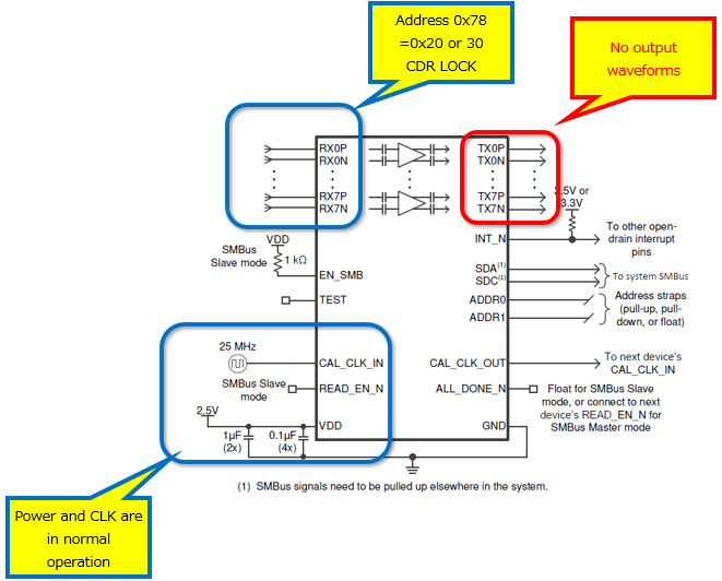
My customer designed the circuit with DS250DF810 which is used for the 25G communication between FPGA and ethernet PHY. My customer is able to confirm the CDR lock on the input side(RX0N, RX0P, ~ RX7N and RX7P), but My customer cannot observe the output waveform on the output side(TX0N, TX0P, ~ TX7N and TX7P). My customer would like to confirm what happens in DS250DF810.
- Are there any registers which show the current situation in DS250DF810?
- Are there any registers which my customer should configure to fix this issue?

Best regards,
Shunsuke Yamamoto

