This thread has been locked.

If you have a related question, please click the "Ask a related question" button in the top right corner. The newly created question will be automatically linked to this question.

SN65DSI84-Q1: SN65DSI84-Q1 Sequence DSI CLK HS mode Issue

Part Number: SN65DSI84-Q1

Hi expert,

The main problem is that during seq2, the DSI CLK is operated in HS mode.

image.png

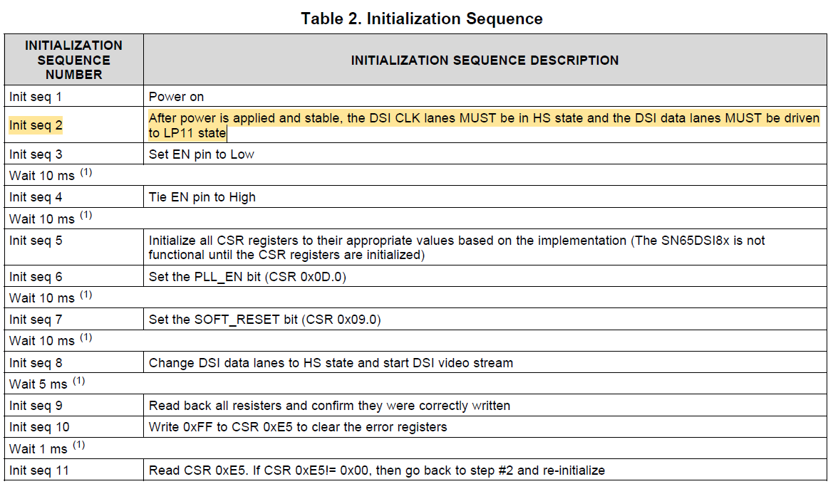
However, seq 2 to 8 do not mention any switching, and in actual SoC operation, there can be cases where the clock transitions from HS back to LP-11.

We believe this situation complies with the DSI MIPI protocol.

In reality, seq8 only imposes requirements on DSI DATA. Furthermore, seq10 and seq11 completed successfully without errors. And the display is normal.

mmexport1769763001243.jpg

I will proceed with the following support needs:

1. Is it acceptable for the clock to go to LP-11 between seq2 and later steps from customer test?

2. If HS CLK is mandatory, is there a way for the DSI to achieve this, and what corresponding mode needs to be set?

3. Can you provide an internal test waveform that meets the requirement of the clock remaining in HS from seq2 onwards?

4. If it is strictly required that after seq2, the clock must enter HS and cannot have any LP-11 periods, but this cannot be achieved at the current stage, are there any workarounds?

Thanks

Xiaoxiang

  • Hi Xiaoxiang,

    Thank you for sharing the details this questions.

    1. The clock has to remain in HS state, it cannot be switched to LP11, unless the device is disabled, or if there is a restart sequence.

    2. The SoC DSI interface can generally be programmed so that it remains in HS state and does not go to LP11 state.

    3. We do not have a waveform from a setup to share here. In HS state, it would remain in HS mode similar to your waveform and it would not enter into LP state.


    4. Could you please check with the SoC datasheets and with the vendor about how to set this up? This is a requirement for the power-up sequence for the DSI84 device and the clock going into LP state can cause blank screen and PLL unlock.

    Did the customer already look into how to change the DSI clock settings? Generally, this can be programmed for the DSI interface.


    Best regards,
    Ikram

  • Hi Ikram,

    Thanks for your support.

    3. We do not have a waveform from a setup to share here. In HS state, it would remain in HS mode similar to your waveform and it would not enter into LP state.

    You can see my waveform that I provided, there is LP in the HS.

    Do you think the waveform I have provided meets the requirements?

    In addition, the customer wants to see the standard waveforms measured, can you provide them? 

    SOC is manufactured by Qualcomm.

    Thanks

    Xiaoxiang

  • Hi Xiaoxiang,

    In the waveforms shared, the HS state DSI clock rate is not clear, and this might be because it's not zooming in enough or because the sampling rate is not high enough for the DSI rate. However, it is going into LP state and this is not meeting the requirements. Since the DSI clock is the source clock in this case, it has to remain in HS mode for continuous clock mode. This is a common D-PHY use-case with continuous clock mode; please check with the SoC documents on how to set this up.

    I do not have an exact waveform for this, but a general DSI waveform is shared in this debugging guide: /cfs-file/__key/communityserver-discussions-components-files/138/DSI-Setup-and-Debugging-Guide-v1.0.pdf

    Note that this document is not specific for the DSI84 and contains information for other use-cases and devices. In the "DSI Waveforms" section, there is an example shared where the DSI clock lane remains in HS mode. The DSI data lanes go into LP state during blanking periods.


    The DSI clock frequency will also depend on the resolution and number of lanes used. Please use this to calculate: [FAQ] SN65DSI84: SN65DSI83, SN65DSI84, and SN65DSI85 resolution guide


    Best regards,
    Ikram


  • Hi Ikram,

    Thank you for your support.

    There is no doubt that the customer's actual operating waveform matches the one you provided.

    Note that this document is not specific for the DSI84 and contains information for other use-cases and devices. In the "DSI Waveforms" section, there is an example shared where the DSI clock lane remains in HS mode. The DSI data lanes go into LP state during blanking periods.

    However, we did not observe the corresponding initialization for the DSI CLK between SEQ2~ SEQ8. You mentioned that the HS (High Speed) mode will not transition to LP11;

    Could you provide an actual measurement from the EVM showing a standard initialization waveform with the DSI CLK stable in HS mode?

    Thanks

    Xiaoxiang

  • Hi Xiaoxiang,

    The DSI example above already shows a waveform of DSI clock remaining in HS state. The example shown is an actual measurement shared in that presentation. This is a common setup with DSI interface, using a continuous clock that remains in HS state.


    The EVM or DSI84 device does not control the this; the DSI source SoC or generator sets the clock to be in HS state. 

    There is no doubt that the customer's actual operating waveform matches the one you provided.

    You mentioned earlier that the customer's DSI clock switches to LP11 state during runtime. It should instead be programmed for continuous clock mode.


    Best regards,
    Ikram

  • Hi Ikram,

    Currently, Harman's software design cannot avoid this brief entry into the LP11 state. However, tests on dozens of boards have not shown any anomalies, so the customer believes this may not pose a significant risk.
    The customer's requests are:
    1. Can you provide the test waveforms of the Golden design for the customer's reference? (I recall this component was from another product line, so the BU may not have the relevant test setup, but could you communicate with the previous HSSC team to obtain the relevant test waveforms to support our conclusions regarding the limitations?)
    2. Alternatively, can you help assess the risk of the customer's current design? Since the project is nearing mass production, they need to confirm the extent of the design risk.
    3. Or, can the BU provide a complete test setup for the customer to perform their own testing and debugging?

  • Hi Alan,

    1 and 2. As we mentioned before, the clock has to be in HS state for continuous DSI clocking if the DSI clock is used as the source. This is a requirement shared in the datasheet, and it can cause PLL unlock if this is not met. These conditions are how the system was validated, and that is why these are shared in the datasheet power-up sequence.

    Continuous clock mode with DSI is a common application, so I would suggest to please check if this can be updated. 

    Otherwise, the other alternative would be to use the REFCLK as LVDS clock input. The REFCLK frequency would need to match exactly so that the LVDS clock frequency would be a multiple of the the REFCLK frequency.


    3. The customer can test the system as it is and check for whether there is any error flags shown in the register map, and if there is any PLL unlock flickering, or blank screen after many power-ups and run times.

    In either case, this would be up to the customer discretion, since from the device requirement's a free-running continuous HS mode clock is required to run with DSI clock as the source.

    Best regards,
    Ikram