SN65CML100: Can SN65CML100 differential input/output withstand 3.3V?

Part Number: SN65CML100
Other Parts Discussed in Thread: DS15BA101, DS90LV004, SCAN90004

Hi,

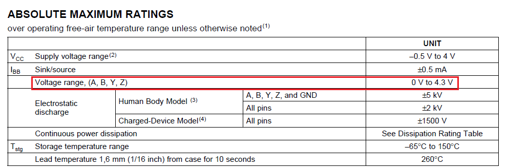
For SN65CML100, can the Differential InputVoltage|VID| and  DifferentialOutputVoltage((OUT+)-(OUT−)) be up to 3.3V? There is only maximum value for input/output not differential pins in the datasheet. Otherwise can this chip use to transmit SGMII signals?

Thank you!

image.png

  • Hello,

    That abas max voltage range you highlighted is measured from pin to GND, which in a normal application will be a combination of the differential and common-mode voltages. 

    The output voltages are given in the Output Electrical Characteristics table. If these do not fit with SGMII, I would recommend AC-coupling the output signal and add your own external DC-bias at the SGMII receiver if needed. 

    Regards,

    Matt

  • Hi Matt,

    Thank your reply, it's helpful. I also want to know the absolute maximum Differential Input Voltage |VID| and  Differential Output Voltage((OUT+)-(OUT−)), shown as below.

    Thank you!

  • Hi Matt,

    I also want to know information about DS15BA101, DS90LV004 and SCAN90004. What are the absolute maximum Differential Input Voltage |VID| and  Differential Output Voltage((OUT+)-(OUT−)) of them, and can these use to transmit SGMII signals?

    Thanks a lot.

  • Hello, 

    I want to clarify that the Absolute Maximum Ratings table int he datasheet specifies the voltage/current range at which the device can operate and not be damaged. However, we do not recommend using these abs max ranges to operate the device since it will cause reliability issues if the device is constantly being stressed to its abs max limit. Instead you should refer to the Recommended Operation Conditions table to understand the ranges at which the device can reliably operate (see below). the max recommended input VID for SN65CML100 is 1V. 

    Again, I am unfamiliar with SGMII signals so I can't make a call on if this device will work with SGMII or not. However, if you have the SGMII driver/receiver thresholds from the devices' datasheet, please share so I can let you know if the device will work or not. 

    Regards,

    Matt 

  • Hi Matt,

    The requirement is that the RX/TX pins should not be damaged when 3.3V disturbance is between RX+ and RX-(or TX+ and TX-). So I need the absolute maximum ratings.

  • Hello,

    There is no defined abs max range for differential input voltage, because differential voltage is not the only factor that makes up the overall single-ended voltage for a pin. You have to factor in common mode voltage as well. If you had 1V common-mode, then your abs max differential voltage would be 2V since the pins cannot handle a negative voltage. If your common-mode voltage was 4V, then your abs max differential voltage would be 600mV since that would cause the single ended voltage to rise to 4.3V. In the image below, the common-mode voltage is VOS, the differential voltage is VOD, and the single ended voltages are VD+ and VD-. Hopefully this helps illustrate the point I'm trying to make. 

    Regards,

    Matt