TCAN4550-Q1: SPI communication issue while reading data from an TCAN4550-Q1.

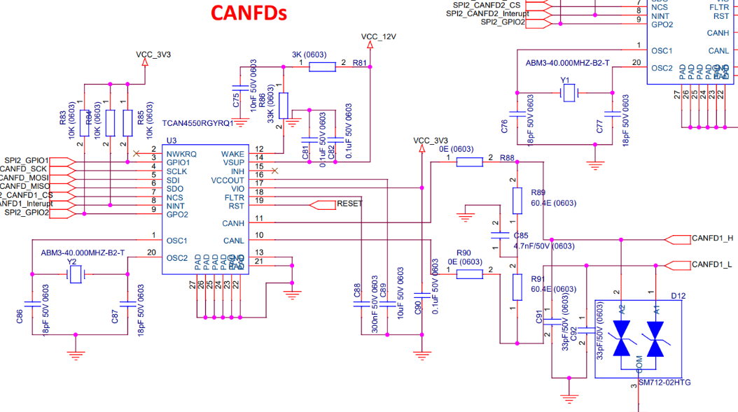
Part Number: TCAN4550-Q1

Hi Texas,

I am facing an SPI communication issue while reading data from an SPI slave device.

During transmission, I can clearly see SCLK and MOSI toggling correctly, and MOSI is sending valid data. However, on the MISO line, I only see noise, and the received data in the RX buffer is always 0x00 or 0xFF.

Here are my SPI configuration details:

SPI Mode: Mode 0 (CPOL = 0, CPHA = 0)

Bit order: MSB first

Baud rate: 15 Mbps

Master mode

Observations:

1.Clock and MOSI are active during transmission

2.MISO does not show valid data

3.RX buffer reads either 0x00 or 0xFF

My questions:

1.Could this be a software configuration issue, or does this indicate a hardware / timing problem?

2.Is 15 Mbps too high for reliable MISO sampling?

3.Under what conditions does the slave actively drive the MISO line?

4. is there modification need on hardware part.

I will share my SPI driver code for review and schematic .
Please let me know what I should verify or change.

Thanks in advance for your support.      main.c image.png

  • Hello Vishnu,

    I don't see anything in the schematic that looks like an obvious error that would prevent SPI communication.  However, it is unclear what the state of the RESET pin is and whether it is High or Low during your test.  The RST pin needs to be LOW during normal operation.  If it is HIGH, then the device will be held in a state of reset and prevent SPI communication.

    Can you measure the voltage levels on the VSUP, VIO, VCCOUT, FLTR, and RST pins when you are trying to communicate through SPI?  There should be a positive voltage on all the supply and filter pins, and RST needs to be low.  (VSUP = 12V, VIO = 3.3V, VCCOUT = 5V, FLTR = 1.5V, RST = 0V)

    The device has a failsafe feature that will cause the device to enter Sleep Mode if it is not configured into Normal Mode or has had the PWRON (Power On) interrupt bit cleared in register 0x0820 within 4 minutes of powering up.  When the device enters Sleep Mode, SPI communication is disabled.

    Normally I would suggest monitoring the INH and NWKRQ pin voltages and an indicator of Sleep Mode, but these pins are not used in your schematic.  Therefore monitoring the VCCOUT and FLTR LDOs for a voltage will indicate if the device has entered Sleep Mode.  If it has entered Sleep Mode, you will need to wake up the device through a Wake Up Pattern (WUP) on the CANH and CANL pins, a Local Wake Up (LWU) pulse on the WAKE pin, pulsing the RST pin HIGH, or power cycling the VSUP supply.

    A SPI rage of 15 Mbps is OK.

    Can you provide the scope or logic analyzer plots of the 4 SPI signals you are monitoring?  If all the voltage levels are correct on the device, then there may be an issue with the SPI signal formatting.  I don't see anything obvious from the code or schematic, so it would help to observe the waveforms for errors.

    Regards,

    Jonathan

  • Hello Jonathan,


    Thank you for the suggestions.

    I measured the voltage levels on the pins while attempting SPI communication, and the readings are as follows:

    VSUP = 11.72 V
    VIO = 3.22 V
    VCCOUT = 0 V
    FLTR = 0 V
    RST = 0 V

    The CS pin goes low during SPI transmission, and the SPI clock and MOSI waveforms look correct on the oscilloscope. However, the MISO line remains at 0 V and no response is observed from the device.

    Based on your explanation, it appears the device may not be entering Normal Mode or may already be in Sleep Mode, since both VCCOUT and FLTR LDO outputs are at 0 V.

    For further debugging, I captured oscilloscope images of the SPI signals (CS, SCLK, MOSI, and MISO) and attached them below.  CS pin properly working. 

    Since VSUP is present at around 11.72 V, could you help me understand why VCCOUT and FLTR are still at 0 V? How can I rectify this condition so the device enters normal operation or standby mode?

    You also mentioned the Local Wake Up (LWU) concept. Could you please explain in more detail how LWU works and how it should be implemented in this setup? can i apply for this instead of  powerup sequence .

    Please let me know if these voltage levels indicate that the device is still in reset or sleep mode, or if there are additional checks you would recommend.


    Regards,
    Vishnu    

  • Hi Vishnu,

    Yes, it appears the transceiver is in Sleep Mode if VCCOUT and FLTR pins are both 0V.  I would suggest you read section 8.4.3 of the TCAN4550-Q1 Datasheet (Link) for more information on Sleep Mode and the different methods to wake up the device.

    There are several methods to wake up the device.

    -  A Wake Up Pattern (WUP) which is a Dominant-Recessive-Dominant pattern on the CAN bus will be detected and cause the device to transition to Standby mode and enable the internal LDOs. 

    - A Local Wake Up (LWU) which is a voltage pulse on the WAKE pin i.e pulling the WAKE pin Low in your application since you have a pull-up resistance to VSUP will also cause the device to transition to Standby mode and enable the internal LDOs. 

    - Toggling the RST pin high is another option

    - Power cycling the VSUP voltage is the last option

    Once you have performed any of these methods, there is a 4-minute timer that starts which is called the Sleep Wake Error (SWE) timer and this is a failsafe feature of the device which ensures the device does not draw power from a low-power system if the device wakes up unintentionally which could drain a vehicle's battery.  Therefore, if the device has not been configured into Normal Mode through a SPI write to register 0x0800[7:6], or the PWRON bit has not been cleared by a write to register 0x0820[20] before the 4-minute SWE timer expires, then the device will transition to the low-power Sleep Mode and disable the internal LDOs.  If this occurs you will need to perform one of the Wake Up Methods I've previously listed.

    So your your setup, you can either pull the WAKE pin at least 3V less than VSUP to create a LOW on this pin that will be detected as a LWU.

    Or you can pulse the RST pin to VIO to create a wake up.

    Lastly, you could drive the CAN bus with a Dominant-Recessive-Dominant pattern or simply send it a CAN message from another node which will have both dominant and recessive bits that will meet the WUP requirements.

    Once the device is awake and in Standby mode, you have 4 minutes to clear the PWRON flag or configure the device and place it into Normal mode before it will return to Sleep Mode.  I would recommend that you always immediately clear the PWRON flag as your first step which will terminate the SWE timer and allow you as much time as you need to configure the device without fear of it returning to Sleep Mode.

    Section 8.4.5 of the datasheet also discusses this Failsafe feature in greater detail.

    Regards,

    Jonathan

  • Hi Jonathan,

    Thank you very much for your support — you helped resolve my issue. The SPI communication is now working properly, and I have confirmed this by successfully reading the Device ID through LWU sequence.

    However, I have one important question. According to the datasheet, after applying power, the device is expected to enter Standby Mode. In my case, the device appears to be entering Sleep Mode instead.

    Could this be due to a schematic-related issue, or does the device default to Sleep Mode under certain conditions? I would like the device to enter Standby Mode or Normal Mode by default after power-up. Is there any recommended configuration or hardware consideration to achieve this?

    Looking forward to your guidance.

    Best regards,
    Vishnu