This thread has been locked.

If you have a related question, please click the "Ask a related question" button in the top right corner. The newly created question will be automatically linked to this question.

DS90UB960-Q1: DS90UB960-Q1 Deserializer: FPD III - Link lock issue

Part Number: DS90UB960-Q1
Other Parts Discussed in Thread: DS90UB935-Q1

Hi team,

We are using DS90UB960-Q1 deserializer and ds90ub935-q1 serializer for on our product in Valeo. 

The deser and our camera serializer are configured to be in synchronous mode - meaning even before configuring the deserialzier after power-up, the link lock should be established between the camera serializer and deser. 

But despite the components being configured to be in sychronous mode, the link lock is not established until the deser configuration is completed.

We would like to get support from TI to debug the issue.

  • Howdy Sahcin,

    With FPD-Link 3, a link is automatically established between the SerDes pair if both devices are strapped to the correct mode. If a link is not established when both devices are powered on, it usually indicates a problem with the mode the devices are operating in.

    A couple questions:

    1. What configuration changes are you making to the deserializer to establish the link between the UB960 and UB935 after initial power up?
    2. If possible, could you share your schematic showing the hardware strap configuration? I would like to confirm that the resistor values are correct for Synchronous mode in both devices.

    Thank you,

    Ethan Woods

  • Hello Ethan 

    Thanks for your reply.

    Mode setting table as per deser datasheet:

    HW Schematics (deser):

    HW schematics (ser):

    For register settings, we are expecting the link lock to happen automatically during powerup even before any configuration is done for the camera serializer and the deserializer. Can you please provide some more info if there is anything specific to be checked for?

  • Howdy Sachin,

    I have reviewed your schematics, and all values look correct in regard to the datasheet specifications for Synchronous mode on the 960 and 935.

    To verify the devices are actually strapping to the correct mode, I would like to know the values in their respective mode registers after initial powerup.

    • For the 960, please provide the value in registers 0x58 (BCC_CONFIG) and 0x6D (PORT_CONFIG). BCC_CONFIG will provide information on the back channel rate depending on the strapped mode. PORT_CONFIG will provide information on the mode the device actually strapped to.
    • For the 935, please provide the value in register 0x03 (MODE_SEL). MODE_SEL will provide information on what mode the device strapped to when the device powered on.

    Additionally, you said the devices did not establish a link until the deserializer configuration was completed. What configurations did you have to change to establish the link between the 960 and 935 after initial power up?

    Thank you,

    Ethan Woods

  • Hello Ethan,

    1. We are checking the register values as you mentioned for 960 and 935 after initial startup. We will share the values shortly

    2. I was checking the values of the same registers values written during configuration of ser-des phase:

    960:

    0x58 (BCC_CONFIG): 0x5E

    0x6D (PORT_CONFIG): 0x7C

    935:

    0x03 (MODE_SEL): 0x10

  • Howdy Sachin,

    For the 960:

    • 0x58 = 0x5E. This value corresponds with the device operating with a back channel speed of 50 Mbps along with enabling I2C_PASS_THROUGH. This back channel speed is correctly configured to operate with the 935 in CSI-2 Synchronous Mode.
    • 0x6D = 0x7C. This value corresponds with the device strapping to CSI-2 Mode correctly along with the default values in 0x6D. This is correct for CSI-2 Synchronous mode.

    For the 935:

    • 0x03 = 0x10. This value corresponds to a mode override into CSI-2 Synchronous Mode. Bit 4 is high (1), which means the register mode will override the strapped value, thus setting the mode into CSI-2 Synchronous Mode (2:0 = 000). I assume the override is done because the strapped value in bits 2:0 is not 000.

    This would be why the link happens after the configuration on the seralizer side, as the strapped value in bits 2:0 are overridden and the mode is set into CSI-2 Synchronous. 

    Hopefully that makes sense. If you are having to override the mode in the serializer (935), then the strapped mode will probably be incorrect. Looking forward to your values upon initial powerup.

    Thank you,

    Ethan Woods

  • Hello Ethan,

    Good day.

    Find below the values from deser 960 for each of the Rx ports just after the initial powerup and before any configuration is written in the deser:


    --- Reading registers for Channel 0 ---
    Value at 0x58 = 0x18

    Value at 0x6D = 0x79


    --- Reading registers for Channel 1 ---
    Value at 0x58 = 0x18
    Value at 0x6D = 0x79


    --- Reading registers for Channel 2 ---
    Value at 0x58 = 0x18
    Value at 0x6D = 0x79


    --- Reading registers for Channel 3 ---
    Value at 0x58 = 0x18
    Value at 0x6D = 0x79

    The FPD3_MODE in 0x6D[1:0] does not seems to be latched to correct mode

    We cannot read the serializer registers since link lock is not available and there is no access to the registers in ser 935.

    Please provide us know if any further debugging is required from our end. If yes, please share the correct steps for debugging the issue.

    Thanks. 

  • Howdy Sachin,

    Thank you for providing the initial register values. For all RX Ports on the Deserializer:

    • 0x58 = 0x18. This corresponds to BC_ALWAYS_ON as 1, which is default and correct. To have a working back channel, this bit must be high. The issue lies in bits 2:0 = 000, which corresponds to a back channel rate of 2.5 Mbps. This value is used for the DVP Serializers 913/933, which have a lower back channel rate. For pairing with the 935 in CSI-2 synchronous mode, the back channel rate needs to be 50 Mbps.
    • 0x6D = 0x79. This corresponds with the correct default values and a strapped FPD3_MODE of RAW12 Low Frequency Mode. This setting is what sets your strapped back channel rate to only 2.5 Mbps, as this is the default value for operating with the 913/933 in DVP mode.

    This means that the mode value the DS90UB960 is strapping to is incorrect. To confirm this, you can measure the voltage at the MODE pin on the DS90UB960 Deserializer to see what value the device is reading after the voltage divider. Given the chosen resistance values (RHigh = 78.7kΩ and RLow = 97.6kΩ), the MODE pin should be receiving a voltage of ~0.996V.

    For reference, based on the mode chart for the 960:

    • For CSI-2 Synchronous Mode: The voltage range is 0.945V-1.0656V. Anywhere inside this range the device will strap to CSI-2 Synchronous Mode.
    • For RAW12 LF Mode: The voltage range is 1.1556V-1.2672V. Anywhere inside this range the device will strap to DVP RAW12 LF Mode.

    Additionally, you can do the same for the DS90UB935 Serializer to check the strapped mode. By measuring the voltage on the MODE pin (which should be 0V, since it is tied to ground), you can identify which MODE the device will strap to.

    Given that the DS90UB960 is strapping to the wrong mode, there are two potential issues:

    • The resistor values are incorrect, causing the voltage at the MODE pin to be outside the range of CSI-2 Synchronous Mode.
    • The 1.8V rail is noisy, which causes the voltage to fluctuate and be at an unstable value when PDB goes high during initial powerup.

    Please let me know any additional questions and concerns.

    Thank you,

    Ethan Woods

  • Hello Ethan,

    sorry for the late reply,

    We measured the voltage on the mode pin in 960 and it measured 0.993V.

    Do you see any issue in the voltage measured that can lead to wrong mode strapping?

  • Howdy Sachin, 

    Thanks for your measurement. This is odd because this voltage corresponds to CSI-2 Synchronous Mode, which the device should strap to.

    Another possible issue is the 100nF capacitor that is parallel to the mode pin. During initial startup, this capacitor needs to charge to full voltage of the divider, which might cause an issue depending on how fast the PDB on the 960 goes high. With a calculated time constant of ~4.36 ms, this could be an issue with the voltage on the pin when PDB is set high.

    Before diving further into potential issues, could you desolder the capacitor and see what register 0x6D returns after powerup? 
    My thought is the device is strapping into RAW12 LF Mode around the ~0.374V range when the capacitor is initially charging. Since the other way to strap into RAW12 LF is above the measured 0.993V, this should not be possible since the divider outputs 0.993V.

    Additionally, could you send a screenshot of your PDB power sequencing in the schematic? If desoldering the capacitor works, then the issue could lie with your PDB pin being pulled high too quickly, causing the mode pin to strap too early.

    Thank you for your patience,

    Ethan Woods

  • Hello Ethan,

    Sorry for the delay.

    We managed to do a couple of test to debug the issue. Please find below our observations:

    1. The MODE pin voltage is taking ~12 to ~13 ms to get to the expected range of 0.993V when the 100nF capacitor is connected. On the the other hand it is only taking ~1.3 ms to reach the expected voltage when the capacitor is not connected.

    KSS2.0 VOL+ B0 sample Risetime Mode Pin DeSer DS90UB960.pdf

    2. We tested setting the PDB PIN high with a delay of  5ms and 10 ms after the ECU powerup as you explained.

    • Tested with a delay of 5ms before PDB
      0x58 = 0x18
      0x5D = 0x7B

      No link lock established

      0x7B = 0111 1011(RAW 10 Mode)

    • when added 10 ms delay before PDB set to high, the mode seems to be set properly

      (R5F2_0)%--- Reading registers for Channel 0 ---
      Value at 0x58 = 0x1E
      Value at 0x6D = 0x7C
      --- Reading registers for Channel 1 ---
      Value at 0x58 = 0x1E
      Value at 0x6D = 0x7C
      --- Reading registers for Channel 2 ---
      Value at 0x58 = 0x1E
      Value at 0x6D = 0x7C
      --- Reading registers for Channel 3 ---
      Value at 0x58 = 0x1E
      Value at 0x6D = 0x7C
      --- Reading registers for Channel 0 ---
      Value at 0x58 = 0x1E
      Value at 0x6D = 0x7C
      --- Reading registers for Channel 1 ---
      Value at 0x58 = 0x1E
      Value at 0x6D = 0x7C
      --- Reading registers for Channel 2 ---
      Value at 0x58 = 0x1E
      Value at 0x6D = 0x7C
      --- Reading registers for Channel 3 ---
      Value at 0x58 = 0x1E
      Value at 0x6D = 0x7C

    So from our analysis it seems like the capacitor might be causing the issue in link lock happening synchronously.

    Can you please provide guidance on how to solve this issue permanently? 

    Will removing the capacitor or using a capacitor with lower capacity help in resolving this?

  • Hi Sachin,

    Thank you for the data. This is what I believed was happening. PDB goes HIGH while the MODE pin is still in a charging state, therefore it straps to the wrong value. This is because when PDB goes HIGH during power-up, it straps the value that is currently on the mode pin.

    The slow charging of the 100nF capacitor is likely due to the large resistance voltage divider that is on the MODE pin. Therefore, the solution would be to have your MODE voltage set before PDB goes high.

    Before removing any capacitors or changing values, could you send the schematic portion of your PDB pin on the 960? As you have shown above, adding delay to the PDB pin (possibly through a different capacitor value) could provide a solution. I would like to verify the hardware you have currently on the PDB pin to control it.

    Another solution would be to just remove the capacitor on the MODE pin. This will ensure the voltage on the MODE pin is HIGH before PDB is HIGH, since PDB will most likely have a capacitor on it. If filtering is needed using this 100nF capacitor on the MODE pin, then I would suggest looking into the behavior of PDB, rather than removing components.

    Note that the typical application diagram in Section 8.2 on the 960 datasheet has a lower capacitor value on the IDx/MODE pins because they will charge faster than PDB.

    Ultimately, the voltage level on the MODE pin must be settled at the desired value by the time PDB goes HIGH. 

    Thank you,

    Ethan Woods

  • Hello Ethan,

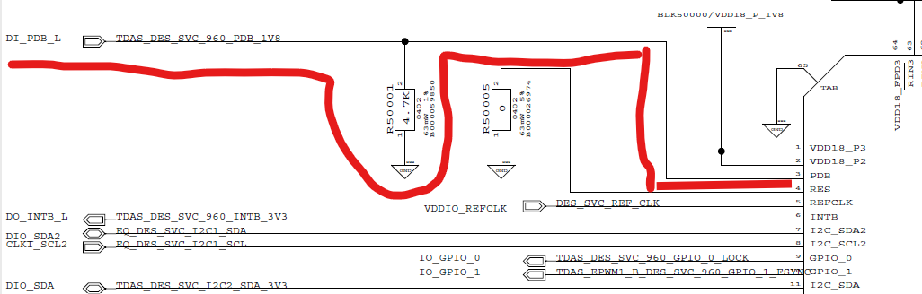
    Please find below the schematic portion of the PDB pin on 960

  • Hi Sachin,

    Thanks for sending the PDB portion of the 960 schematic.

    This tells me that the PDB signal is software controlled, so there are no hardware alterations we can make to delay its rise time.

    So that leaves two solutions:

    • Delay PDB rise time via software and monitor resulting power-up sequence to ensure nothing is incorrect.
    • Modify/remove the capacitor on the MODE pin to ensure a quicker rise time of the MODE voltage. By using a lower capacitor value, this should decrease the time it takes for the MODE voltage to reach its full value of .993V. Additionally, removing the capacitor completely will also decrease the time it takes for the MODE pin to reach its desired voltage.

    Note that the large resistor values that create the voltage divider on the MODE pin also slow the charging rate of the capacitor. By having larger resistance values in the divider, a smaller current is driven through the MODE pin, resulting in a higher charge time of the capacitor. If the capacitor filtering is needed, then I would recommend to either add additional delay on the PDB software or lower the capacitor value on the MODE pin. These changes should allow for your voltage on the MODE pin to be settled before PDB goes HIGH.

    Best regards,

    Ethan Woods

  • Hello Ethan,

    How are you?

    Thanks for your solution proposals. We are looking into the feasibility of the solutions from our end.

    Just a couple of points to clarify for TI:

    1. What is the preferred capacitor value for the MODE pin? We could see a value of 0.1uF in Figure 8-4. Typical Connection Diagram (Coaxial). Is this the recommended value for the MODE pin? And do we have to follow this capacitor with 0.1uF which is 100nF?                    
    2. If, it is ok to change the capacitor to mitigate our issue with link lock, can we use 1nF or 10nF capacitor? Do you foresee any impact while moving to a lower capacitor than what is recommended as per the image above? IF yes, what capacitor value do TI recommend?

     we would like to get your opinion on the 2 points before deciding if any hardware change can mitigate the issue.

    Parallelly we are looking into the possibilities of increasing the delay in the PDB pin activation via Sw.


  • Hello Sachin,

    I am doing fantastic this Monday morning. Thanks for asking. Hope all is well on your side as well.

    The capacitor on the MODE pin is not an explicit REQUIREMENT for our devices, as it is just used for some additional noise filtering on the MODE pin. Some iterations of our datasheets have this capacitor in the Typical Application, while some others do not. With this being said, it is up to you to decide whether you want to keep it, lower it, or completely remove it. I want to note that if changing the capacitor value, any lower than 1 nF or higher than 0.1 uF will have diminishing value where it will not do much to impact the noise on the MODE pin, if any. If a lower capacitor value can help to mitigate the issue with strapping to the correct voltage, changing the value to a lower capacitance such as 10 nF or 1 nF is acceptable.

    Best,

    Ethan Woods