This thread has been locked.

If you have a related question, please click the "Ask a related question" button in the top right corner. The newly created question will be automatically linked to this question.

TPD1E01B04: Inquiry Regarding PCB Assembly Conditions

Part Number: TPD1E01B04

Hello Team, 

My customer has several questions regarding the PCB assembly of TPD1E01B04DPLT. 

1. Assembly precautions
Are there any specific conditions or precautions that should be considered during PCB assembly for this device?

2. Recommended PCB surface finish
Regarding PCB surface finishes, the customer is considering the following options:

  • Pre-flux treatment
  • ENIG (electroless nickel immersion gold)
  • Lead-free HASL

Could you please advise which surface finish is recommended for assembling this device?

3. Photos of mounted device / acceptance criteria
If available, could you please share photos of the device after assembly (top view and side view)?

Since this device does not have side electrodes, the customer understands that fillet formation is difficult.
If possible, we would appreciate it if you could also provide examples of OK / NG assembly conditions as judged by TI.

4. Inspection method for solder joint quality
Could you please advise how the solder joint condition should be verified? For example:

  • Visual inspection (what solder appearance would be acceptable)
  • X-ray inspection (acceptable contrast / void appearance)
  • Electrical testing, etc.

5. Review of actual assembly condition
The customer has attached photos of their actual assembly condition.
They are concerned that the solder volume may be excessive.

Could you please share your opinion on this, and also advise on possible countermeasures or improvements if applicable?
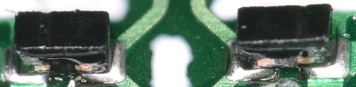
image.png

Thank you very much for your support.

Best regards,

Maia

  • Hi Maia, 

    Let me check with our manufacturing and packaging team to see if they have any insight on soldering our devices. I will reach back out once I have more information. 

    Best,

    McKenzie

  • Hello McKenzie,

    I hope you are doing well.

    I would like to follow up on my previous inquiry and ask if there are any updates regarding the current support status.

    If there is any additional information needed from my side, please let me know.

    Thank you very much for your support.

    Best regards,
    Maia

  • Hello McKenzie,

    I hope you are doing well.

    I would like to follow up on my previous inquiry and ask if there are any updates regarding the current support status.

    If there is any additional information needed from my side, please let me know.

    Thank you very much for your support.

    Best regards,
    Maia

  • Hi Maia, 

    I am still wanting to hear back on precautions and photos. 

    For the question about solder joint inspection, I would say most customers use X-ray inspection. It can be difficult for small, leadless packages like this one.

    For recommended surface finish, our devices can work with many different finishes. I would recommend doing what is best for your project and application. 

    Best,

    McKenzie

  • Hi McKenzie,

    Sorry to follow up again.
    Could you please let me know if there are any updates regarding the precautions and photos?

    If it is difficult to obtain them, could you please share any useful application notes instead?

    Best regards,
    Maia

  • Hi Maia, 

    No worries! For precautions, the main thing will be the tilt of the diode after soldering. A tilt can happen across the long-axis due to the small size of the package. This is normal but some customers are initially concerned by it. To manage tilting, it is best to follow the stencil design and control the amount of solder paste. Too much solder paste can lead to higher amounts of tilting.

    I am still waiting on photos. I will try to get those to you this week. 

    Best,

    McKenzie

  • Hi McKenzie,

    Thank you for the additional information!

    I will share it with the customer.
    I also look forward to receiving the photos.

    Best regards,

    Maia

  • Hi McKenzie,

    Could you please provide an update on the situation since then?

    Best regards,

    Maia

  • Hi Maia, 

    I have some pictures but they aren't the highest quality due to the package being so small. But I did want to share this image below. 

    So based on the images you provided in your first post, it looks like the device being soldering like the first picture. Is the correct stencil and land pattern being used? Looking at one of the pictures I took, you can't see solder at all which means it is fully under the device. 

    Best,

    McKenzie