This thread has been locked.

If you have a related question, please click the "Ask a related question" button in the top right corner. The newly created question will be automatically linked to this question.

DS90UB941AS-Q1EVM: Inquiry on how to output Analog LaunchPAD Script using DS90UB941AS-Q1EVM.

Part Number: DS90UB941AS-Q1EVM
Other Parts Discussed in Thread: DS90UB941AS-Q1

Dear TI SerDes FAE

I am a H/W engineer who develops AVN products.


DS90UB941AS-Q1EVM: I would like to run the Color Bar Pattern Generator by connecting the DS90UB941AS-Q1EVM to the monitor that has the DS90UB948TNKDRQ1 applied. - Interface forum - Interface - TI E2E support forums


I received support through the link above about two months ago. 

Due to internal development delays, progress has been somewhat delayed, but we are now trying to output the script according to the values ​​set in the DS90UB941AS-Q1EVM using the pattern generator of the Analog LaunchPAD.

But I don't know how to use the function to extract scripts based on the item values ​​set in the pattern generator.

Please tell me how to output a script with values ​​set in the pattern generator.

1.png

2.png

Please reply. 


  • Hi Kisuk,

    Thank you for reaching out. Yes I can create a script for you based on the resolution you provided. Are you using single or dual FPD-Link? Are you planing to use incoming SuperFrame as well or single image?

    Aaron

  • Dear Aaron Heng

    Thank you for your quick response.
    First of all, I was wondering how to output the values set in the DS90UB941AS-Q1EVM environment as a script, so I am grateful that you said you would write it.
    The connection concept for the board we're developing will consist of two cases, as shown in the figure below.
    Please refer to it.

    If my explanation is insufficient or missing anything, please let me know.

    Thank you.

    LCD Use Case 1 (There are cases where only one LCD is used.)

    LCD Case1

    LCD Use Case 2 (Sometimes two LCDs are used.)

    LCD Case2

  • Hi Kisuk,

    Thanks for sharing the diagram. I will review it and provide you the initialization script by tomorrow.

    Aaron

  • Hi Kisuk,

    Please see attached script and try it on your system for case 1. Let me know if it is working or not. Once I got the confirmation from you. I will work on case 2.

    import time
    Ser_addr = 0x18
    
    time.sleep(0.5)
    board.WriteI2C(Ser_addr,0x01,0x08) # Reset
    board.WriteI2C(Ser_addr,0x01,0x02) # Reset
    
    board.WriteI2C(Ser_addr,0x3,0xDA) #Passthrough I2C
    
    time.sleep(0.5)
    board.WriteI2C(Ser_addr,0x5B,0x00) #Auto-detect 
    
    board.WriteI2C(Ser_addr,0x1E,0x01) #Select FPD-Link III Port 0 for registers access
    board.WriteI2C(Ser_addr,0x66,0x1A)
    board.WriteI2C(Ser_addr,0x67,0x01) #M=1
    board.WriteI2C(Ser_addr,0x66,0x03)
    board.WriteI2C(Ser_addr,0x67,0x03) #N=3
    
    #Program Video Timing
    board.WriteI2C(0x18, 0x66, 0x04) #THW and TVW
    board.WriteI2C(0x18, 0x67, 0x00)
    board.WriteI2C(0x18, 0x66, 0x05)
    board.WriteI2C(0x18, 0x67, 0x91)
    board.WriteI2C(0x18, 0x66, 0x06) 
    board.WriteI2C(0x18, 0x67, 0xD9)
    board.WriteI2C(0x18, 0x66, 0x07) #AHW and AVW
    board.WriteI2C(0x18, 0x67, 0x80)
    board.WriteI2C(0x18, 0x66, 0x08)
    board.WriteI2C(0x18, 0x67, 0x07)
    board.WriteI2C(0x18, 0x66, 0x09)
    board.WriteI2C(0x18, 0x67, 0x2D)
    board.WriteI2C(0x18, 0x66, 0x0A) #HSW
    board.WriteI2C(0x18, 0x67, 0x28)
    board.WriteI2C(0x18, 0x66, 0x0B) #VSW
    board.WriteI2C(0x18, 0x67, 0x02)
    board.WriteI2C(0x18, 0x66, 0x0C) #HBP
    board.WriteI2C(0x18, 0x67, 0x28)
    board.WriteI2C(0x18, 0x66, 0x0D) #VBP
    board.WriteI2C(0x18, 0x67, 0x02)
    
    board.WriteI2C(Ser_addr,0x65,0x04) #using internal timing and internal clock
    board.WriteI2C(Ser_addr,0x64,0x15) #enable PG/color bars
    
    
    board.WriteI2C(Ser_addr,0x1E,0x01) #Select FPD-Link III Port 0
    board.WriteI2C(Ser_addr,0x07,0x58) #0x07,0x58
    board.WriteI2C(Ser_addr,0x08,0x5C) #0x08,0x5c
    board.WriteI2C(Ser_addr,0x03,0x9A) #0x03,0x9A Enable I2C_PASSTHROUGH, FPD-Link III Port 0
    
    board.WriteI2C(Ser_addr,0x01,0x00) #Release DSI

    Aaron

  • Dear Aaron Heng
    Thank you for writing the script for case 1.
    I'll forward it to our software developers to see if it works and get back to you.
    Thank you.

  • Hi Kisuk,

    No problem. Take your time whenever you are ready to share the results. Once it it worked, I will make another script for case 2.

    Aaron

  • Dear Aaron Heng

    After delivering the script to the S/W developer, I received the following feedback.
    (Currently, we are testing the script on a board we're developing, not the EVM.)
    Please review and see if you have any guidance.

    1)  Pattern Generation Success by doing additional work

    Since the pattern was not output with the code and PG Register value you provided, I did additional work as follows.


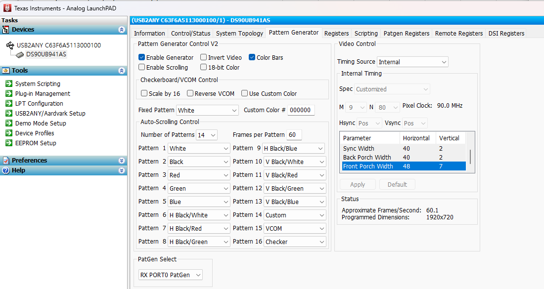
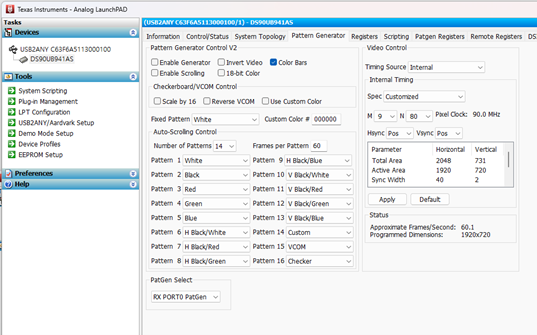
    I used the Pattern Generator to input 1920x720 60Hz display timing information. Then, I set M=9, N=80 to generate a DSI 90MHz clock.

    Timing Information

    Total Area          2048, 731

    Active Area         1920, 720

    Sync Width             40,   2

    Back Porch Width   40,  2

    Front Porch Width  48,  7


    I compared the dumped register values ​​below with the script code that sent them, changed the values, and added all unset registers.


    2)  How to configure MIPI input to output through SER?

    The setup information is as follows:

    2-1) MIPI Information

    Port0 default
    MIPI use 4 lanes, PHY data rate = 540mbps

    panel bpp = 24

    DSI Freq = 90MHz

    2-2) Display Timing Information

                               Hor / Ver

    Total Area          2048, 731

    Active Area        1920, 720

    Sync Width             40,   2

    Back Porch Width   40,  2

    Front Porch Width  48,  7


    Do you need any additional information?

    ※ The modified script attachment file is missing, so I am attaching it again.

    PGRegister_DumpApply_941AS_1920_720_Internal_Patgen_89p58Mhz.zip

    Thank you.

  • Hi Kisuk,

    It’s great that you were able to bring up the pattern generator.

    Next, you need to calculate the TSKIP value. After that, make sure to disable the pattern generator so that the incoming video from the source can pass through to the 981.

    Use the following formula:

    TSKIP_CNT = Round(65 × f(DSI) − 5)

    Note that you must divide the calculated value by 2 before programming the register, since the register applies a left shift internally.

    Aaron

  • Dear Aaron Heng

    After conveying the information you provided to the S/W developer, we are conducting various tests, but it seems that the MIPI input to DS90UB941AS-Q1 is not being output properly.

    Could you please provide some guidance on the following inquiry from our S/W developer? Please review it.

    <Inquiries>

    We converted our TCC8070 U-Boot bring-up sequence into the TI evaluation-board style board.WriteI2C() format for easier review.
    The sequence is based on our current DS90UB941AS C implementation, using non-splitter / Port0 / 4-lane / 90 MHz pixel clock.
    We are currently using:
    • Serializer address: 0x0C
    • Serializer alias: 0x58
    • Remote deserializer actual address: 0x58
    • Remote deserializer alias: 0x5A
    • Touch actual/alias address: 0x34 / 0x34
    Please review whether:
    1. Please review the code flow, register setup sequence, values, and register configuration order.
    2. the reset sequence (value: 0x02 -> register: 0x08 vs value: 0x07 -> register: 0x08) is correct,
    3. GENERAL_CFG = 0xDA -> GENERAL_CFG = 0x9A is required,
    4. deserializer alias 0x5A needs additional programming beyond 0x06/0x07/0x08
    5. TSKIP value 0x18 is appropriate for our DSI clock condition. But DSI_FREQ(0x5F) is read as 91MHz
    6. The code in the attached file adds TSKIP_CNT and some registers to the sequence provided by TI.

    <CODE> - The code file was not added as an attachment, so I added it to the main text.

    import time

    # --------------------------------------------------------------------
    # Device Address
    # --------------------------------------------------------------------
    serAddr = 0x0C # DS90UB941AS_I2C_ADDR, serializer local I2C address
    desAddr0 = 0x58 # remote deserializer actual address (8-bit format)
    desAlias = 0x5a # remote deserializer alias (8-bit format)
    touchAddr = 0x34 # remote touch actual address (8-bit format)
    touchAlias = 0x34 # remote touch alias address (8-bit format)

    # --------------------------------------------------------------------
    # Display Condition
    # --------------------------------------------------------------------
    # Pixel Clock = 90 MHz
    # DSI clock = PCLK * 24 / (2 * # of DSI lanes)
    # = 90 * 24 / (2 * 4)
    # = 270 MHz
    # DSI input port 0
    # 4 lanes DSI
    # Non-splitter / Forced Single mode

    # --------------------------------------------------------------------
    # 1) Reset / Disable DSI input
    # --------------------------------------------------------------------
    board.WriteI2C(serAddr, 0x01, 0x02) # RESET_CTL = DIGITAL_RESET1 (0x02)
    time.sleep(0.01)

    board.WriteI2C(serAddr, 0x01, 0x08) # RESET_CTL = DISABLE_DSI_INPUT (0x08), DSI input disabled

    # --------------------------------------------------------------------
    # 2) General configuration / I2C pass-through preparation
    # --------------------------------------------------------------------
    board.WriteI2C(serAddr, 0x03, 0xDA) # GENERAL_CFG = 0xDA, initial I2C pass-through related setup

    # --------------------------------------------------------------------
    # 3) Force single-link mode (non-splitter)
    # --------------------------------------------------------------------
    board.WriteI2C(serAddr, 0x5B, 0x01) # DUAL_CTL1 = FPD3_TX_MODE_FORCED_SINGLE (0x01)

    # --------------------------------------------------------------------
    # 4) Select Port0 specific register set
    # --------------------------------------------------------------------
    board.WriteI2C(serAddr, 0x1E, 0x01) # TX_PORT_SEL = 0x01, select FPD-Link III Port0 specific registers

    # --------------------------------------------------------------------
    # 5) Bridge control: DSI Port0 / continuous clock / 4 lanes
    # --------------------------------------------------------------------
    board.WriteI2C(serAddr, 0x4F, 0x8C) # BRIDGE_CTL = 0x8C
    # bit7 DSI_CONTINUOUS_CLK = 1
    # bit[3:2] DSI_LANES = 4 lanes
    # DSI_PORT_SEL = Port0

    # --------------------------------------------------------------------
    # 6) DSI_CONFIG_1 : HSYNC / VSYNC polarity
    # --------------------------------------------------------------------
    board.WriteI2C(serAddr, 0x40, 0x04) # IND_ACC_CTL = INDSEL_DSI_PORT0_DIGITAL (0x04)
    board.WriteI2C(serAddr, 0x41, 0x21) # IND_ACC_ADDR = DSI_CONFIG_1 (0x21)
    board.WriteI2C(serAddr, 0x42, 0x60) # IND_ACC_DATA = DSI_POLARITY_HS_VS_HIGH (0x60)

    # --------------------------------------------------------------------
    # 7) DPHY_SKIP_TIMING : THS-SKIP / TSKIP_CNT
    # --------------------------------------------------------------------
    # TSKIP_CNT(dec) = Round(65 * fDSI(GHz) - 5)
    # fDSI = 0.2688 GHz
    # TSKIP_CNT = 12
    # DPHY_SKIP_TIMING[6:1] = 12 => register value = 0x18
    board.WriteI2C(serAddr, 0x40, 0x04) # IND_ACC_CTL = INDSEL_DSI_PORT0_DIGITAL (0x04)
    board.WriteI2C(serAddr, 0x41, 0x05) # IND_ACC_ADDR = DPHY_SKIP_TIMING (0x05)
    board.WriteI2C(serAddr, 0x42, 0x18) # IND_ACC_DATA = TSKIP_CNT value (0x18)

    # --------------------------------------------------------------------
    # 8) Internal DSI clock settings (datasheet power-up sequence)
    # --------------------------------------------------------------------
    board.WriteI2C(serAddr, 0x40, 0x10) # IND_ACC_CTL = INDSEL_DSI_ANALOG_PLL (0x10)
    board.WriteI2C(serAddr, 0x41, 0x86) # IND_ACC_ADDR = 0x86
    board.WriteI2C(serAddr, 0x42, 0x0A) # IND_ACC_DATA = 0x0A
    board.WriteI2C(serAddr, 0x41, 0x94) # IND_ACC_ADDR = 0x94
    board.WriteI2C(serAddr, 0x42, 0x0A) # IND_ACC_DATA = 0x0A

    # --------------------------------------------------------------------
    # 9) Remote I2C mapping for Port0
    # --------------------------------------------------------------------
    board.WriteI2C(serAddr, 0x1E, 0x01) # TX_PORT_SEL = 0x01, Port0 specific register bank

    # 0x06 : DES_ID_DES_ID_1
    # bits[7:1] = remote deserializer actual address
    # bit[0] = FREEZE_DEVICE_ID
    # deserializer actual address = 0x58 (8-bit format), FREEZE_DEVICE_ID = 0
    board.WriteI2C(serAddr, 0x06, 0x58) # DES_ID_DES_ID_1 = 0x58

    # 0x07 : SlaveID_0
    # bits[7:1] = remote touch actual address
    board.WriteI2C(serAddr, 0x07, 0x34) # SlaveID_0 = 0x34

    # 0x08 : SlaveAlias_0
    # bits[7:1] = remote touch alias address
    board.WriteI2C(serAddr, 0x08, 0x34) # SlaveAlias_0 = 0x34

    # --------------------------------------------------------------------
    # 10) General configuration final mode
    # --------------------------------------------------------------------
    board.WriteI2C(serAddr, 0x03, 0x9A) # GENERAL_CFG = 0x9A, final pass-through/control mode

    # --------------------------------------------------------------------
    # 11) Enable DSI input
    # --------------------------------------------------------------------
    board.WriteI2C(serAddr, 0x01, 0x00) # RESET_CTL = ENABLE_DSI_INPUT (0x00), normal operation
    time.sleep(0.02)

    # --------------------------------------------------------------------
    # 12) Optional sanity check
    # --------------------------------------------------------------------
    # DSI_FREQ register (0x5F) can be read back for DSI pixel frequency indication
    # Example:
    # dsiFreq = board.ReadI2C(serAddr, 0x5F)
    # print("DSI_FREQ =", hex(dsiFreq))
    #
    # Why is disFreq read as 91MHz ?

  • Hi Kisuk,

    No worries. I will review this script and get back with you by Monday. 

    Aaron

  • Dear Aaron Heng,

    Do you happen to have any advice regarding the inquiry from our software developer that we requested a review of?

    I would appreciate it if you could confirm.

    Thank you.

  • Hi Kisuk,

    Apologies for the delay in my response.

    First, I would suggest not defining an alias for the serializer, as mentioned in the note. I also recommend keeping all deserializer and I2C secondary addresses the same for both physical and alias addresses.

    I checked the T_SKIP value and calculated it to be 30. Could you please share your equation for how you arrived at a value of 12? You may also need to apply a shift by 2.

    Additionally, could you please read registers 0x64 and 0x65 on the main page and share the values?

    Aaron

  • Dear Aaron Heng

    We are sharing the software developer's response to your question. Please refer to it when providing further advice.


    1. The requested register values are follows.
    [ub941] PGCTL(0x64) = 0x10
    [ub941] PGCFG(0x65) = 0x00

    2. he process by which the TSKIP_CNT values 0x18, 0x1A, and 0x1E (30) are derived is as follows.
    It varies depending on the minute difference in PCLK values and the interpretation of the definition of fDSI.
    PCLK was set by assuming two values of 89.6 or 90 MHz, fDSI was assumed to be 270 MHz, and DPHY Data Rate was assumed to be 540 MHz. It was assumed that 2 bits are transmitted per clock.

    1) When Pixel Clock = 89.6 MHz
    TSKIP_CNT = Round(65 × fDSI(GHz) − 5)
    DPHY_SKIP_TIMING register uses TSKIP_CNT in bits[6:1].

    Assumption:
    - Pixel Clock = 89.6 MHz
    - DSI lanes = 4
    - DSI clock = PCLK × 12 / lanes

    Calculation:
    DSI clock = 89.6 × (12 / 4) = 268.8 MHz
    fDSI = 268.8 MHz = 0.2688 GHz

    TSKIP_CNT = Round(65 × 0.2688 − 5)
    65 × 0.2688 = 17.472
    17.472 − 5 = 12.472
    Round(12.472) = 12

    TSKIP_CNT = 12

    12(dec) = 0x0C
    0x0C << 1 = 0x18

    Final result:
    TSKIP_CNT = 12
    DPHY_SKIP_TIMING = 0x18

    Comment:
    This result follows the TI reference script assumption:
    fDSI = PCLK × 12 / lanes.
    With this interpretation, the calculated DPHY_SKIP_TIMING value is 0x18.


    2) When Pixel Clock = 90 MHz

    TSKIP_CNT = Round(65 × fDSI(GHz) − 5)

    Assumption:
    - Pixel Clock = 90 MHz
    - DSI lanes = 4
    - DSI clock = PCLK × 12 / lanes

    Calculation:
    DSI clock = 90 × (12 / 4) = 270 MHz
    fDSI = 270 MHz = 0.270 GHz

    TSKIP_CNT = Round(65 × 0.270 − 5)
    65 × 0.270 = 17.55
    17.55 − 5 = 12.55
    Round(12.55) = 13

    TSKIP_CNT = 13

    13(dec) = 0x0D
    0x0D << 1 = 0x1A

    Final result:
    TSKIP_CNT = 13
    DPHY_SKIP_TIMING = 0x1A

    Comment:
    Using the same TI reference script assumption
    (fDSI = PCLK × 12 / lanes),
    a slightly higher pixel clock of 90 MHz gives TSKIP_CNT = 13,
    so DPHY_SKIP_TIMING becomes 0x1A.


    3) When fDSI = 540 MHz = 0.54 GHz

    Assumption:
    - Pixel Clock = 90 MHz
    - DSI lanes = 4
    - fDSI is interpreted as:
    fDSI = PCLK × 24 / lanes

    Calculation:
    fDSI = 90 × 24 / 4 = 540 MHz = 0.540 GHz

    TSKIP_CNT = Round(65 × 0.540 − 5)
    65 × 0.540 = 35.1
    35.1 − 5 = 30.1
    Round(30.1) = 30

    TSKIP_CNT = 30

    30(dec) = 0x1E
    0x1E << 1 = 0x3C

    Final result:
    TSKIP_CNT = 30
    DPHY_SKIP_TIMING = 0x3C

    Comment:
    In this case, fDSI is interpreted as the per-lane bit rate
    (fDSI = PCLK × 24 / lanes).
    With this interpretation, the calculated DPHY_SKIP_TIMING value becomes 0x3C.


    4) Summary:
    The difference between 0x18, 0x1A, and 0x3C comes from how fDSI is defined.

    - If fDSI = PCLK × 12 / lanes:
    - PCLK = 89.6 MHz -> DPHY_SKIP_TIMING = 0x18
    - PCLK = 90 MHz -> DPHY_SKIP_TIMING = 0x1A

    - If fDSI = PCLK × 24 / lanes:
    - PCLK = 90 MHz -> DPHY_SKIP_TIMING = 0x3C

    We would like to confirm which fDSI definition should be used for
    DS90UB941AS THS-SKIP (DPHY_SKIP_TIMING) calculation in our use case.


    <This is an additional inquiry.>

    5) The DSI_FREQ_P1 Register (Address = 0x5F) is read as 91.
    We calculated TSKIP_CNT based on 90MHz (13) and set the value of the DPHY_SKIP_TIMING Register (Offset = 0x5) to 0x1A (13<<1 --> 0x1A), but DSI_FREQ reads a value corresponding to 91MHz. What is the problem?

    6) When establishing (initializing) the connection of mipi_dsi input to DES via SER,

    the DES_ERROR field value of the GENERAL_STS Register (Address = 0xC) is 1.

    The DES_ERROR field value is also 1 when outputting to the display via PAT_GEN.

    What is the meaning of DES_ERROR being set to 1, and what is the cause? Are there any register values or settings that need to be reset or examined when DES_ERROR is 1?

    Thank You.

  • Hi Kisuk,

    Thank you for confirming the register settings.

    Based on my understanding, you would first calculate the pixel clock (PCLK) as:
    PCLK = 2048 × 729 × 60.

    Then, to determine the DSI frequency (fDSI), use:
    fDSI = (PCLK × 24) / DSI lanes.

    Next, apply the T_SKIP formula:
    T_SKIP = round(65 × fDSI (GHz)) − 5.

    After that, you will need to apply a left shift by 2.

    Could you also confirm the incoming frequency from the source (in this case, the SoC)?

    Best regards,
    Aaron

  • Dear Aaron Heng

    Please refer to the reply containing information confirmed by the software developer regarding the matter you mentioned.


    1. using your method, TSKIP_CNT is
    PCLK = 2048 × 729 × 60 = 89.57 MHz (90 MHz approx..)
    fDSI = (PCLK × 24) / DSI lanes = ( 89.6 x 24 ) / 4 = 537.6 --> 0.5376
    fDSI = (PCLK × 24) / DSI lanes = ( 90 x 24 ) / 4 = 540 --> 0.54

    T_SKIP is 30, 30 << 1 = 0x3C

    Does the calculated fDSI 540 value mean that the MIPI DSI CLK input value should be 540MHz?

    Currently, I am inputting 270MHz as shown in the waveform below.

    2. But, 941AS TI’s Register Manual page 40 says


    fPCLK = fDSI * N(DSI Lanes) / 12
    fDSI = (fPCLK x 12) / N(DSI Lanes)
    T_SKP is 18, 18 << 1 = 0x1A

    3. Which of the two methods is correct?

    4. Measured mipi-dsi CLK
    - (in development) Telechips 8070 SOC mipi-dsi CLK is 270MHz

    <MIPI DSI CLK_P>

    Thank you.

  • Hi Kisuk,

    According to your oscilloscope measurements, it appears that the DSI source is currently programmed to 270 MHz, which is half of the theoretical value. Therefore, you will need to program the DSI source to 540 MHz instead of 270 MHz.

    Please also ensure that the system is operating in continuous clock mode. I recommend using the method I previously shared to calculate both the PCLK and fDSI.

    Hope this helps. Please let me know if you have any additional questions.

    Aaron

  • Dear Aaron Heng

    Thank you for always being so kind and helpful.

    In order to reflect what you mentioned, we are receiving FAE support from the AP company (Telechips) to change the MIPI DSI CLK from 270MHz (current) to 540MHz (planned), and I have a few questions.

    1) I am curious why the MIPI DSI CLK needs to be 540MHz.

    According to the LGD panel specifications, the PCLK required for a 60Hz refresh rate is approximately 90MHz, and the MIPI lane-specific Data Rate required for this PCLK timing is 540MHz.

    fDSI = (PCLK × 24bpp) / DSI lanes = ( 90 x 24 ) / 4 = 540 MHz

    As the MIPI D-PHY standard uses DDR CLK processing 2 data symbols per clock cycle, the settings per PHY Lane are CLK 270MHz and Data 540MHz, which satisfy the panel's 60Hz refresh rate.

    Therefore, shouldn't the MIPI CLK be 270MHz and the Data be 540MHz to meet the D-PHY specifications?

    Question : Are you perhaps referring to the case where two LCDs are connected (Use Case 2) as the reason why the CLK must meet 540MHz?

    (Currently, the test is being conducted with only one LCD connected.)

    I would appreciate it if you could confirm.

    Thank you.

  • Hi Kisuk,

    You may want to refer to the MIPI DSI specification if you want more detail information. Here is the example how to program the MIPI DSI clock on the host side, you usually work backward from the display timing.

    1. Find the pixel clock
      PCLK = H_{total} x V_{total} x FPS
      This is the same general timing method used in display timing examples.
    2. Convert pixel clock to DSI lane rate
    3. Convert lane rate to DSI clock

    So the practical formula is:

    DSI clock = (PCLK x BPP) / (2 x N_{lanes})

    For example RGB888, 4 lanes:

    DSI clock = PCLK x 24} / (2 x 4} = 3 x PCLK

    That means:

    • If PCLK = 89.58 MHz, then DSI clock ≈ 268.74 MHz
    • per-lane data rate is 537.48 Mbps/lane.

    Hope this helps. Let me know if you have additional questions.

    Aaron

  • Dear Aaron Heng

    There is confusion during the process of discussing the issue you mentioned with the AP supplier.
    Please cross-check the following information.

    Based on the response you provided this time, isn't the MIPI DSI CLK speed I measured and reported last week normal?

    Last week, I inquired whether the settings were correct as the current MIPI DSI clock was measured at approximately 270 MHz. However, since you advised that it should be set to 540 MHz, there seems to be some confusion.

    Currently, the MIPI DSI clock is set to approximately 270 MHz, and the data transfer rate is set to approximately 540 Mbps per lane.

    It seems I configured it correctly, so this is strange.
    Please double-check that there are no issues with the settings based on the two cases below.

    Use Case 1)
    When inputting one MIPI DSI group (1 clock lane + 4 data lanes) into the DS90UB941AS and connecting it to a single monitor via one FPD LINK port.

    Is it correct to use a clock frequency of approximately 270 MHz per lane and a data bandwidth of approximately 540 Mbps?


    Use Case 2)
    When inputting one MIPI DSI group (1 clock lane + 4 data lanes) into the DS90UB941AS and connecting it to two monitors via two FPD LINK ports.

    Is it correct to use a clock frequency of approximately 540 MHz per lane and a data bandwidth of approximately 1080 Mbps?

  • Hi Kisuk,

    I wish I can read Korean. Please help translate the posted. Thank you.

    Aaron

  • Dear Aaron Heng

    I apologize. It seems I made a mistake by copying and pasting from Google Translate.

    I have corrected the text by translating the original text back into English.

    Thank you.

  • Hi Kisuk,

    Yes, your understanding is correct which programming NRZ at 270 MHz corresponds to 540 Mbps.

    Please note that the MIPI DSI configuration may vary depending on whether you are using single-port or dual-port mode. Single-port mode supports up to 105 MHz PCLK, while dual-port mode can support up to 210 MHz PCLK. Therefore, the MIPI DSI frequency should be programmed based on your target resolution and the selected port configuration.

    Hope this helps. Please let me know if you have any questions.

    Aaron