This thread has been locked.

If you have a related question, please click the "Ask a related question" button in the top right corner. The newly created question will be automatically linked to this question.

AM62P: DP83867 Link Up Failure: AM62P based board

Part Number: AM62P
Other Parts Discussed in Thread: DP83869, , SYSCONFIG

We are developing a custom board based on the TI AM62P5 SoC with a DP83867 Gigabit Ethernet PHY connected via RGMII interface. We are running Linux 6.6.58-ti (Yocto-based). We have successfully established MDIO communication and the PHY is detected correctly, but we are unable to bring up the Ethernet link. Trying to connect using working ethernet cable and connection.
 
Current Progress : 
MDIO communication : Working 
PHY ID detected : 0x2000a231
PHY reset GPIO : Working
Reference clock : 25MHz external
 

Dmesg Logs : 

[    1.260593] am65-cpsw-nuss 8000000.ethernet: initializing am65 cpsw nuss version 0x6BA01903, cpsw version 0x6BA81903 Ports: 3 quirks:00000006
[    1.273629] am65-cpsw-nuss 8000000.ethernet: initialized cpsw ale version 1.5
[    1.280762] am65-cpsw-nuss 8000000.ethernet: ALE Table size 512
[    1.287385] am65-cpsw-nuss 8000000.ethernet: CPTS ver 0x4e8a010d, freq:500000000, add_val:1 pps:0
[    1.301285] am65-cpsw-nuss 8000000.ethernet: set new flow-id-base 19
[    3.389924] systemd[1]: /etc/systemd/system/sync-clocks.service:11: Standard output type syslog is obsolete, automatically updating to journal. Please update your unit file, and consider removing the setting altogether.
[   10.111895] am65-cpsw-nuss 8000000.ethernet eth0: PHY [8000f00.mdio:00] driver [TI DP83867] (irq=POLL)
[   10.147878] am65-cpsw-nuss 8000000.ethernet eth0: configuring for phy/rgmii-id link mode

PHY Register values : 

root@am62pxx-evm:~# phytool read eth0/0/0x00
0x1140
root@am62pxx-evm:~# phytool read eth0/0/0x01
0x7949
root@am62pxx-evm:~# phytool read eth0/0/0x02
0x2000
root@am62pxx-evm:~# phytool read eth0/0/0x03
0xa231
root@am62pxx-evm:~# phytool read eth0/0/0x06
0x0064
root@am62pxx-evm:~# phytool read eth0/0/0x10
0x5048
root@am62pxx-evm:~# phytool read eth0/0/0x11
0x0002

Settings for eth0:
        Supported ports: [ TP    MII ]
        Supported link modes:   10baseT/Half 10baseT/Full
                                100baseT/Half 100baseT/Full
                                1000baseT/Full
        Supported pause frame use: Symmetric
        Supports auto-negotiation: Yes
        Supported FEC modes: Not reported
        Advertised link modes:  10baseT/Half 10baseT/Full
                                100baseT/Half 100baseT/Full
                                1000baseT/Full
        Advertised pause frame use: Symmetric
        Advertised auto-negotiation: Yes
        Advertised FEC modes: Not reported
        Speed: 10Mb/s
        Duplex: Half
        Auto-negotiation: on
        master-slave cfg: forced slave
        master-slave status: unknown
        Port: Twisted Pair
        PHYAD: 0
        Transceiver: external
        MDI-X: Unknown
        Supports Wake-on: ubgs
        Wake-on: d
        SecureOn password: 00:00:00:00:00:00
        Current message level: 0x000020f7 (8439)
                               drv probe link ifdown ifup rx_err tx_err hw
        Link detected: no

root@am62pxx-evm:~# ethtool -i eth0
driver: am65-cpsw-nuss
version: 6.6.58-ti-01497-ga7758da17c28-d
firmware-version:
expansion-rom-version:
bus-info: 8000000.ethernet
supports-statistics: yes
supports-test: no
supports-eeprom-access: no
supports-register-dump: yes
supports-priv-flags: yes


root@am62pxx-evm:~# ls -la /sys/bus/mdio_bus/devices/
drwxr-xr-x    2 root     root             0 Oct  9 15:18 .
drwxr-xr-x    4 root     root             0 Oct  9 15:18 ..
lrwxrwxrwx    1 root     root             0 Oct  9 15:18 8000f00.mdio:00 -> ../../../devices/platform/bus@f0000/8000000.ethernet/8000f00.mdio/mdio_bus/8000f00.mdio/8000f00.mdio:00

 
  • Hi Sarang, 

    I share the below inputs in another thread. Can you verify the same and add your inputs.

    There is a difference in strap value used 

    Not sure if this is an issue but would recommend matching the data sheet or EVM.

    In can the Reset pin is not functional, you could do a reset using the registers as below and test.

    Inputs related to Resetting the EPHY, pin strapping and reading the status

    EPHY strapping 

    Performing EPHY reset 

    7.6.1 Basic Mode Control Register (BMCR)

    7.6.2 Basic Mode Status Register (BMSR)

    Regards,

    Sreenivasa

  • Hi Sreenivasa,

    We are getting voltage RX_CTL pin is 0.019V (19mV) when Rhi(R70)-5.6k & Rlo(R71)-2.4k. Do we need any settings in processor? as per divider it should be 0.99V. Not sure why it is dropping. 

    We did all above setting but still not establishing connection.

  • Hello Ashutosh, 

    You need to probe the voltage level during power cycle.

    Can you please reset the EPHY using the above command and also read the registers value.

    For the above please ensure the reset is pulled high and the SOC reset input is isolated.

    Regards,

    Sreenivasa

  • Hi Shree,

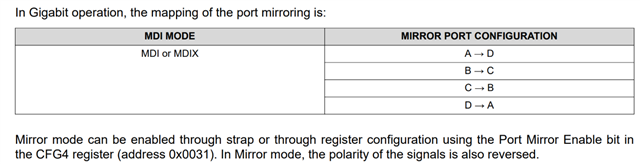
    We found that after reading phytol read eth0/0/0x0e we are getting 0x1031. It means that PHY is going in port mirror enable mode. After clearing this bit, PHY is able to setup the link. Do you know from SW side or HW side how we can setup the correct strap settings so that port mirroring should be disabled at PHY initialization?

    Thanks.

    Rega

    Regards,

    Ashutosh

  • Hello Ashutosh, 

    Thank you for the inputs and good to know the Ethernet interface is working.

    Most of the above inputs i provided are for the EPHY. 

    Can you please start a new thread related to configuring the mirror mode for the EPHY team to support.

    I will review the data sheet and add any inputs i may have.

    Regards,

    Sreenivasa

  • Hello Ashutosh, 

    Can you confirm LED_O status.


    Can you force the pin to be low.

    The EPHY team may be able to further support.

    Regards,

    Sreenivasa

  • Hi Shree,

    Thanks for feedback! now we are able to communicate through ethernet after reading phytol read eth0/0/0x0e we are getting 0x1031. It means that PHY is going in port mirror enable mode. After clearing this bit, PHY is able to setup the link. Now getting IP assignemnet and able to pin to 8.8.8.8 Do you know from SW side or HW side how we can setup the correct strap settings so that port mirroring should be disabled at PHY initialization?

    Also Do we need Exact Values of Resistor for RX_CTL as mentioned in datasheet as per below. as we set later 6.2K & 2.4K but still auto negotiation is yet to start. Is it so sensitive for the values of resistor? Do we need any other settings?

  • Hello Ashutosh, 

    Thank you.

    Also Do we need Exact Values of Resistor for RX_CTL as mentioned in datasheet as per below. as we set later 6.2K & 2.4K but still auto negotiation is yet to start. Is it so sensitive for the values of resistor? Do we need any other settings?

    I suspect you may have to use the recommended values with 1% tolerance components.

    You may be able to check the pin strap status by reading EPHY register.

    For the LED_0 you may want to connect a 2.2K resistor externally.

    Regards,

    Sreenivasa

  • Hello Ashutosh, 

    I added a few pin strap related E2Es.

    (+) DP83867IR: Regarding straps and modes for DP83867 RGMII - Interface forum - Interface - TI E2E support forums

    As I am looking at their schematic, I noticed they are not using the right strapping resistor value, can we please ask them to use the correct strap resistor value?

    DP83867 strap resistors

    DP83869 strap resistors

    You can use the schematic checklist to quickly find the correct strap configuration.

    DP83867 schematic checklist

    slvrbn1a.zip

    DP83869 schematic checklist

    6866.snlr051b.zip

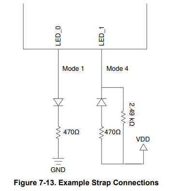
    For DP83867 LED, if a given strap input is resistively pulled low then the corresponding output is configured as an active high driver. In the context of the 4-level straps, this occurs for modes 1, 2, and 3. Conversely, if a given strap input is resistively pulled high, then the corresponding output is configured as an active low driver. In the context of the 4-level straps, this occurs only for mode 4. Below is the LED example for DP83867 and DP83869.

    We also required the turn ratio for the transformer to be +/-@5%. I noticed that the transformer they are using has a +/-5% turn ratio. Please ask them to switch to a different transformer.

    (+) DP83867IS: Strapped Address: Troubleshooting - Interface - INTERNAL forum - Interface - INTERNAL - TI E2E support forums

    PHY address has two strap pins set with the strap ratios in table 7-5:

    It seems like these strap pins are being pulled high by something else connecting to the line. In the customers examples, both cases show that any strap set to mode 1 is strapped into mode 2 somehow. This would cause a strapped address of 0x1 to become 0x5, and a strapped address of 0x8 to become 0x9.

    Are the connected MII MAC receivers pulling these lines high?

    • If so, one potential fix is to add a pulldown resistor on these strap pins when you want to use mode 1. You could try leaving a 2.49k or 10k pulldown on the pin you want to strap to mode 1. 

    Regards,

    Sreenivasa

  • Hello Ashutosh, 

    Checking if you have been to make progress.

    Regards,

    Sreenivasa

  • HI Shree,

    Thanks for the reply! Yes, we have ordered resistor to match with Datasheet to verify the operation of PHY. If it will not work, then pln is to clear the bit from SW at the time of initialization & then it is working. I will update to you once we will match the circuit as per EVM. Also, we need one spin which may delay to upate this one. but thanks for your inputs. for now, everything is working fine.

    Thanks.

    Regards,

    Ashutosh

  • Hello Ashutosh, 

    Thank you.

    Also, we need one spin which may delay to upate this one

    Understand. Please request a schematic review request when the updates are done and before board build.

    I will for now close the thread.

    Regards,

    Sreenivasa

  • Hello Ashutosh, 

    Wanted to check if you had a chance to do some further tests.

    Regards,

    Sreenivasa

  • Hi Sri,

    I have added resistors as per datasheet but no response from PHY for Automatic detection. need to clear bit from SW then its working.

    For now, we have updated schematic & shared to Wang for the review to produce REV-B proto. Can you please verify that schematic if possible.

    Thanks.

    Regards,

    Ashutosh

  • Hello Ashutosh, 

    Thank you.

    I have added resistors as per datasheet but no response from PHY for Automatic detection. need to clear bit from SW then its working.

    I suspect this is something related to EPHY or release of reset.

    May be the EPHY team can help.

    Regards,

    Sreenivasa

  • Hello Ashutosh, 

    I received the schematic.

    I will have a look and comeback if i have some questions.

    Regards,

    Sreenivasa

  • Hello Ashutosh, 

    I had a look at the schematics i received and observed that the MMC1_CLK has a 100R series resistor.

    Can you confirm if you validated the board with the 100R series resistor.

    I see you are using a fixed 3.3V for the SD card data and CMD pullups. I do not see power switch used for the SD card.

    Can you help confirm if you need UHS-I SD card support.

    Regards,

    Sreenivasa 

  • Hi Sri,

    Yes, we have used series resistor for the MMC1_CLK. it is working fine for now. This circuit is from REV-A validate on the boards.

    Do you have any recomandation?

    Thanks.

    Regards,

    Ashutosh

  • Hello Ashutosh

    Thank you.

    The series resistor is provided for control of possible signal reflections.

    TI recommends provisioning for s series resistor 0R initially and adjust (22R) after testing.

    100R could affect the slew as well as the amplitude.

    Regards,

    Sreenivasa

  • Hello Ashutosh

    Can you confirm you do not need higher speed UHS-I SD card support.

    The present configuration seems to be for legacy speed.

    Is the SD card only for internal debug?

    Regards,

    Sreenivasa

  • Hi Sri,

    Noted, we will update resistor to 22E.

    SD card is for only to update or download the code for testing purpose does not use in production.

    No further use in application.

    Thanks.

    Regards,

    Ashutosh

  • Hello Ashutosh

    Thank you.

    Noted, we will update resistor to 22E.

    Please start with 0R.

    I am reviewing the schematic and wanted to check if there are specific sections to focus.

    Regarding the bootmode configuration, i see all the resistors (pullup and pulldown) mounted. 

    Any the resistors required decided during assembly?

    Regards,

    Sreenivasa

  • Hello Ashutosh

    Please note the change above - value changed to 0R.

    regarding the USB interface, can you please confirm the interface configuration for USB0 and USB1

    USB0 - Host or Device 

    USB1 - Host as device

    I do not see the VBUS connected for USB1 and Hence checking.

    VBUS connection is required when the USB interface is configured as device.

    VBUS connection is optional when USB interface is configured as host.

    Regards,

    Sreenivasa

  • Hello Ashutosh

    Regarding the VPP_1V8 supply can you p[lease confirm you used and external supply and also intend to use external supply is production.

    Connecting the 1.8V on board supply is not allowed or recommended.

    An external supply or an on-board LDO with option to be enabled only when eFuse is programmed.

    Please refer the Am62P SK for the VPP LDO implementation.

    Regards,

    Sreenivasa

  • HI Sri, 

    1. We will set the bootmode options to emmc by default at the time of production. for now, debug purpose we are changing manually and adjusting so added all.

    2. Regarding USB, we used USB0 as main device & USB1 as host. USB1 is just to sharing data to external devices, in this case do we need to pull high USB1_VBUS. or we can leave open? kindly suggest.

    3. for secure boot programming we will be providing external supply at the time of production. for now, just added testing purpose. in this case only 1.8V external is required or after bootup we need to provide it?

    Thanks.

    Regards,

    Ashutosh

  • Hello Ashutosh

    For the VPP supply you have the caps and discharge resistor - this should be Ok.

    Make sure you use an IO from the SOC to control the timing.

    For the SD_CLK there is a 47K pullup and a 10K pulldown.

    Can you please confirm you DNId the pullup while testing.

    Regards,

    Sreenivasa

  • Hello Ashutosh

    Missed answering the USB VBUS question

    VBUS connection through a resistor divider is recommended for the USB device configuration.

    USB VBUS connection is optional for the USB host configuration.

    Regards,

    'Sreenivasa

  • Hi Sri,

    SD card pullup & pulldown remain same as per schematic while testing the board.

    I will verify EVM schematic for the USB.

    Thanks.

    Regards,

    Ashutosh

  • Hello Ashutosh

    Thank you.

    Please DNI the pullup 47K in the SD card for all the future tastings.

    Regards,

    Sreenivasa

  • Hi Sri,

    Do we need to DNP all resistors or only from Data lines?

    Thanks.

    Regards,

    Ashutosh

  • Hello Ashutosh

    Thank you.

    This is for SD_CLK only

    Please refer below:

    SD_CLK

    Delete or DNI pullup R84 47K

    R127 10K pulldown is provided

    Regards,

    Sreenivasa

  • Hello Ashutosh

    Thank you.

    Can you help me understand if here are any sections you want me to focus as part of the review.

    Regards,

    Sreenivasa

  • Hi Sri,

    From schematic wise we are ok, we need support on Thermal management support for now SOC is getting heated, so do you have any heatsink recommendation? from Software side we have got information that which peripherals to be shut off those are not using in our application.

    Do you have any suggestion for heatsink? right now using 14X14X10 mm but still going temp. around ~113deg.cel. we have heght and width limitation as 10X20mm

    Thanks.

    Regards,

    Ashutosh

  • Hello Ashutosh

    Thank you for the inputs.

    I will review the schematics and share any comments i may have.

    FYI, i shared a few above.

    Do you have any suggestion for heatsink? right now using 14X14X10 mm but still going temp. around ~113deg.cel. we have heght and width limitation as 10X20mm

    I understand Christopher Roberts is supporting with the analysis.

    Regards,

    Sreenivasa 

  • Hello Ashutosh

    Quick question:

    In the design, i see x4 UARTs being used

    For the UART TX there is a pullup for UART3, UART4 that is expected.

    UART1 and UART2 does not have a pullup for the TX

    Checking if there is a reason for not using external pull?

    Regards,

    Sreenivasa

  • Hi Sri,

    Missed to add. Do we require it? I hope we will be having internal pullup.

    Thanks.

    Regards,

    Ashutosh

  • Hello Ashutosh

    Thank you.

    I suspect this is recommended to ensure the attached device does not float until the host software configures the SOC IO pulls.

    I will add the comment to the PDF schematics  i am reviewing.

    Regards,

    Sreenivasa

  • Hi Sri,

    Can you please share all comments we want to freeze our layout by today.

    Thanks.

    Regards,

    Ashutosh

  • Hello Ashutosh

    Thank you.

    There are ~100+ review comments.

    The Hierarchical schematic drawing is taking additional time to trace and review.

    Please send me a private message to share.

    Regards,

    Sreenivasa

  • Hello Ashutosh

    I have done my best to review the schematics.

    There may be some similar implementation that may need to be updated.

    Please use the below general guidelines along with the review comments.

    We now have an excel that lists the processor power pins and also the connection made in the relevant SK.
    e2e.ti.com/.../faq-am625-am623-am620-q1-am62l-am62a-am62p-am62d-q1-am64x-am243x-custom-board-hardware-design---processor-pin-mapping-and-sk-board-connections-supply-rail-capacitors-and-ferrites
    The recommendation is for customer to do a review of the supply connections before board build using the excel

    Use the latest revision of collaterals
    e2e.ti.com/.../faq-am625-am623-am620-q1-am62l-am62a-am62p-am62d-q1-am64x-am243x-design-recommendations-custom-board-hardware-design---current-data-sheet-revision-updates-revision-backup-and-usage-notes

    AM62x
    Refer the Errata for the supported features by different silicon revision for choosing the required OPN

    Below are some general guidelines that are recommended to be followed during custom board design
    General Notes (For customer to review)
    1.SOC or processor - means the sitara processor used in the design
    2.Attached device - means DDR or flash memory, communication interface, sensors or other external devices interfaced to the processor
    3.We reviewed the schematics to the best. Since the implementation and design flow is customer specific, there may be similar updates that customer will have to review and make the updates.
    4.Verify all the core, analog and IO supplies for the SOC are connected to the recommended supply voltage levels
    5.Verify all the peripheral core, analog and IO supplies for the SOC are connected through ferrite filter
    6.Ensure all the pullups connected to the SOC are pulled up to the correct I/O voltage (matches with the IO supply referenced for the specific IO groups)
    7.Verify the device selection section of the data sheet based on the requirement to confirm the device selection
    8.Verify the pin configuration for the memory interface, communication and IO interfaces using the sysconfig - pinmux tool
    9.Verify the mapping of the schematics symbol pin number and name with the pin name and number as per the pin attributes section of the data sheet
    10.Any SoC pad that has a trace connected and not being actively driven needs an external parallel pull
    11.Verify Device specific Errata for allowed bootmode configuration and erratas affecting the functionality
    12.Verify Pin connectivity table of the data sheet for connecting any unused pins or peripherals including supplies
    13.Please read through the SOC data sheet pin connectivity requirements and ensure the recommendations are followed
    14.When Adjustable DC/DC or LDO are used, verify the resistor divider ration matches the required output voltage
    15.Resistor divider tolerance for discrete DC/DC or LDO output supply feedback is 1% for improved output accuracy
    16.Note the I2C interface exceptions and pin connectivity requirements
    17.Add provision to isolate and probe the OBSCLK for testing
    18.Recommendation is to always perform simulations on the custom board
    19.The system designer must use the IBIS model of each device connected to a signal and the PCB signal trace extractions in a simulation environment to determine the rise/fall time of any signal being sourced by AM62x or other processors
    20.3T caps are used to optimize the use of caps and optimize the PCB look inductance.

    Processor power Pin Mapping Errors
    Ensure the symbol name matches the ball name
    Ensure the net name and the processor signal name matches
    Verify the pin mapping, signal mapping matches the required functionality using the sysconfig pinmux tool

    Processor Signal Pin Mapping errors
    The selected pin can be muxed to the required functionality
    Slected pins follows the IOSET grouping as required
    Selected pin has specific connectivity requirements (pulldown enabled or Open-drain) and has been addresed in the schematic

    SK/EVM design reuse
    1.The SK schematics included some optional components that are configured as DNI
    2.When customers modify the SK/EVM schematics as part of the custom board design, there will be change in the page numbers as well as reference designator numbers
    3.The DNI configuration for the reference designators are reset during this design phase
    4.The recommendation is to refer the SK/EVM PDF schematics for the DNI components and make the required updates

    Notes related to I2C and SPI
    1.Open-drain output type I2C interface - a pullup is required irrespective of IO usage or configuration
    2.Open-drain output type I2C interface - does not support high speed when the IO supply and the I2C signals are connected to 3.3V
    3.Connecting 3.3V to IO supply group and connecting 1.8V supply to IO is not allowed
    4.SPIx_CLK a series resistor recommended when used as SPI clock output
    5.SPIx_CLK add a pull down for the clock input near to the attached device clock input pin

    Notes on software SDK version
    1.In case the project is a new platform, please ensure the latest SDK is used.
    2.In case the project is a derived project using older version/revision, the recommendation is to review the changes (release notes) with respect to the version used vs latest. Based on the changes observed, the required discretion (approach) could be followed - Example: updating any of the drivers of interest (Reach out to the TI applications team through E2E)


    Common SOC LVCMOS IO interface guidelines (For customers to review and make updates)
    1.A number of the SOC IOs are not fail-safe. No external input is recommended to be applied before the processor supply ramps
    2.Processor LVCOMOS IOs have slew rate requirements specified, applying a slow ramp input or connecting a cap at the input is not recommended
    3.Connecting a cap load >22pF at the LVCMOS IO output is not recommended. DNI the cap or perform simulations based on the use case.
    Processor IO buffers (TX(output) and RX(input) and internal pulls (pullup and pulldown)) are turned off during Reset and after reset. A parallel pull is recommended near to the attached device being driven by the processor IO that can float (to prevent the attached device inputs from floating until driven by the host).
    4.A parallel pull (47KΩ) is recommended for any processor IO (pad) that has a trace connected and not being drive actively). When adding parallel pull is not feasible, ensure the traces are routed away from noisy signals
    5.Connecting processor IOs that can be configured for alternate function, directly to supply or ground is not allowed or recommended (including boot mode inputs). Custom board can have an configuration issue with the firmware and mis-configures these LVCMOS IOs that were intended to be inputs, to be outputs driven logic high instead.
    6.Verify cap loading of the SOC output (when any cap value >22 pF (use case dependent, max value) is connected, recommendation is to simulate), slew rate of the input signal (LVCMOS input slew should be 1000 ns or less)
    7.The recommendation is to verify IO level compatibility between the processor IOs (inputs) and the attached device IOs (output)
    8.Provide provision for external ESD protection when external IOs are connected directly to processor inputs
    9.Ensure ST_EN bit in the PADconfig register is enabled for all the IOs
    10.Ensure the pullup or pulldown value used for processor IOs are > 4.7KΩ
    11.Ensure either pullup or pulldown is populated for processor IOs, When provision for pullup and pulldown is provided, place the resistors as tripad

    Regards,

    Sreenivasa

  • Hello Ashutosh,

    Can you please confirm the receipt of the schematics over chat.

    Regards,

    Sreenivasa

  • Hello Ashutosh,

    Can you please confirm the receipt of the schematics over chat.

    Regards,

    Sreenivasa

  • Hi Sri,

    Received.

    Thanks.

    Regards,

    Ashutosh

  • Hello Ashutosh,

    Thank you for the note.

    Regards,

    Sreenivasa

  • Hello Ashutosh,

    Quick check on the eMMC interface

    Can you please confirm if you need to use HS400 speed in the design?

    Regards,

    Sreenivasa

  • Hello Ashutosh,

    The recommendation is to add the OPN for the processor on the schematics.

    FYI, only -Q1 supports HS400

    Regards,

    Sreenivasa

  • Hi Sri,

    we are using HS200 for now & no plan to use HS400. I hope it is just the device change for HS400?

    Thanks.

    Regards,

    Ashutosh

  • Hello Ashutosh,

    Thank you.

    The Q1 parts support HS400.

    There are some specific layout considerations for supporting the HS400.

    I added the app note link in the reviewed schematic i provided to Brian 

    Regards,

    Sreenivasa