


Part Number: DP83867IR
hi expert
1. The network port using the DP83867IRRGZ chip exhibited transmission errors, resulting in packet loss on the lower-level device.
2. Through hardware measurement of the FPGA TXC and TXCTL signals, the following phenomena were observed:
(1) When the TXC clock phase is 2ns ahead of the TXCTL, no packet loss occurs. The waveform diagram measured by the oscilloscope is as follows.
 (2) When the TXC clock is aligned with the TXCL, a large number of packet losses occur. The waveform graph measured by the oscilloscope is as follows

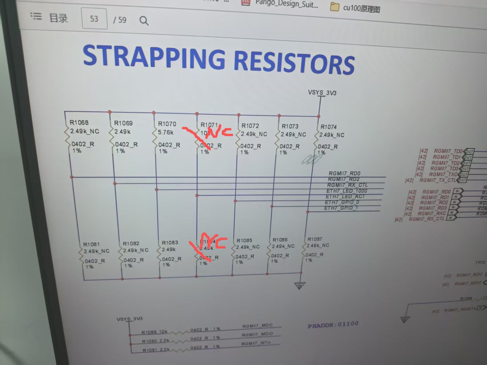
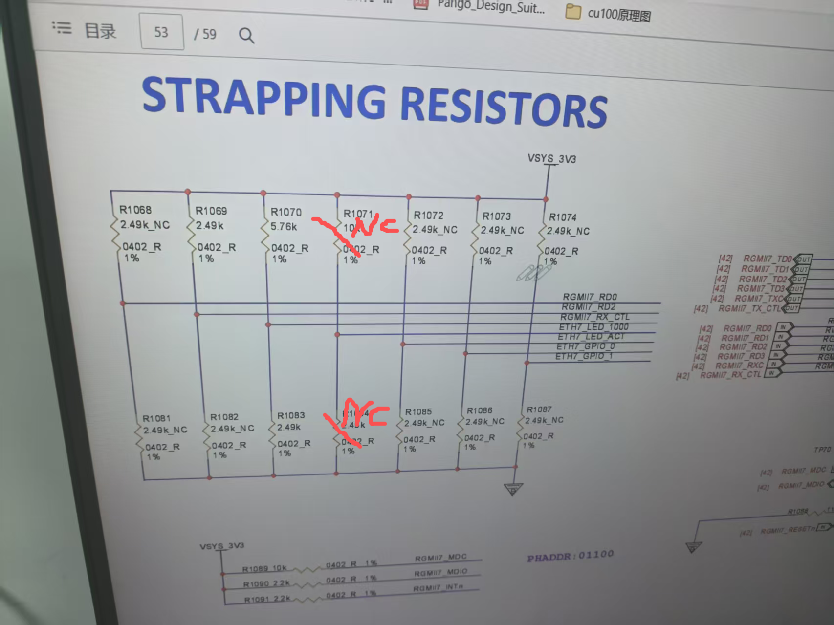
3. The FPGA sends data to the PHY chip. The internal delay within the TX is configured as 2ns. Theoretically, sending along the same edge is correct. This issue needs to be confirmed with you (the Strap resistors of LED1 and LED2 are in the "not connected" state).
Could you please clarify this for us? Specifically, which sequence should we follow when adjusting the RGMII transmitter? And why is the second approach not feasible?
