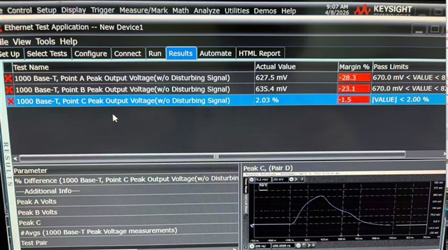
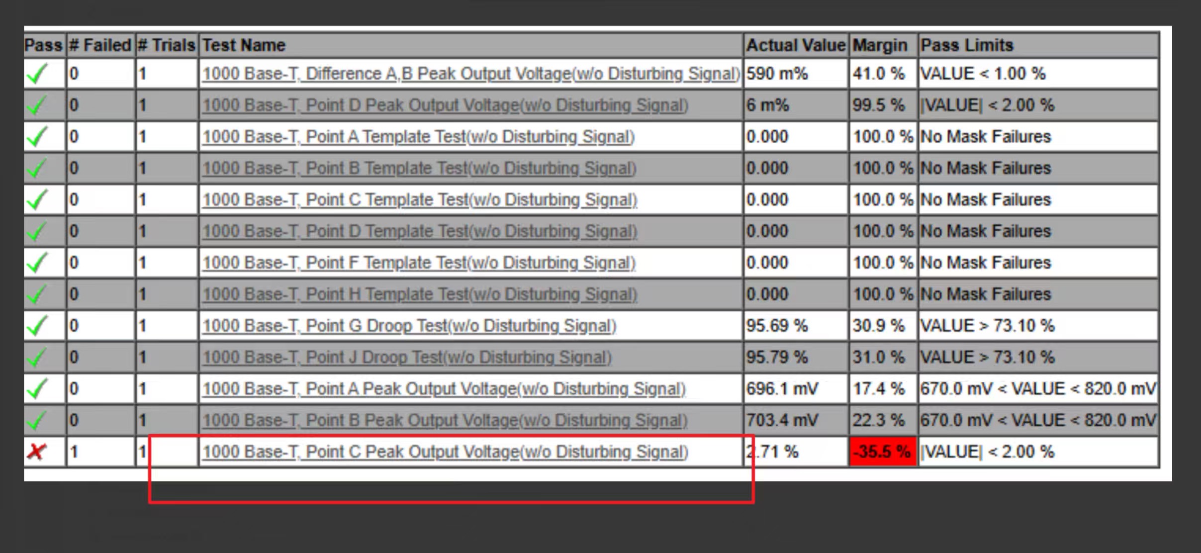
Part Number: DP83867E
Hi team,
My customer is using DP83867 in their system but meet some SI test issue. Can you help to check how to improve?
Below is the SI test and schematics:
BRs,
Rannie
Part Number: DP83867E
Hi team,
My customer is using DP83867 in their system but meet some SI test issue. Can you help to check how to improve?
Below is the SI test and schematics:
BRs,
Rannie