This thread has been locked.

If you have a related question, please click the "Ask a related question" button in the top right corner. The newly created question will be automatically linked to this question.

PCA9534A: Power On Reset Control and Input Capacitance

Part Number: PCA9534A
Other Parts Discussed in Thread: PCA9534,

Hello,

I am working on a design where I have inherited this circuit for an IO expander that controls power supply enable signals. The current part in the design is the NXP PCA9534, and is being replaced with the TI PCA9534.Screenshot 2026-03-18 122729.png
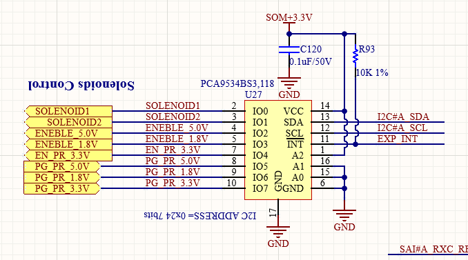
During a forced shutdown on the device where in the supply power to Vcc is killed using a pushbutton interrupt to disconnect the device from the battery, the enable lines A02, A03, and A04 (per the naming convention of the TI component's datasheet) from the IO expander are actually held high. 

Testing has shown that the lines are not held at 3.3V as intended but held at 1V-1.2V. The enable lines are connected to 100k-ohm pull-down resistors at the input to the power supply they feed (SMPS LTC3521EUF#PBF). I believe the issue with the circuit lies in the timing of the POR for the IO expander. 

The input capacitance of C120 would have a time constant of ~1ms, so full discharge around 5ms. I was concerned this might be too fast for the ramp times for rising and falling and may have caused the A0# pins to float/stall as some middle state, but I don't know how this would occur with push-pull outputs on those pins. I tested increasing the capacitance to slow it down, but this did not resolve the issue, indicating my analysis was wrong. 

Is there anything you can think of that would explain this behavior.

Best Regards,

Gavin Birch


  • Hi Gavin,

    A02, A03, and A04

    When you refer to these pins, are you referring to the address pins A2/A1/A0 or the I/O pins: P0/P1/P2...P7?

    Testing has shown that the lines are not held at 3.3V as intended but held at 1V-1.2V. The enable lines are connected to 100k-ohm pull-down resistors at the input to the power supply they feed (SMPS LTC3521EUF#PBF). I believe the issue with the circuit lies in the timing of the POR for the IO expander. 

    I am not sure I understand this prompt. Where is 3.3V being applied? Where is 1V-1.2V being measured at? What pins are the 100k pull-down resistors connected to? 

    Regards,

    Tyler

  • Hello Tyler,

    Sorry for the confusion. I must have grabbed the pin names from the NXP datasheet and not the TI datasheet. I am referring to the I/O pins. 

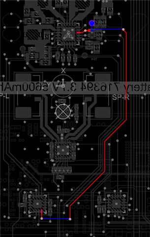
    The 3.3V being applied is the logical high output being set at the I/O pins for 4, 5, 7 on the PCA9534A. During a shutdown event in our design, the voltage at these pins, measured at the downstream device (the reference SMPS) is between 1.04V and 1.26V across the dozen or so measurements I have taken. The 100k pull-down resistors are located at the EN pins of the SMPS roughly 0.5-inches in trace length from the IO expander and are placed between the EN line and GND on the board.

    This is an example of one of these enable traces running from the IO Expander to the SMPS. I would have liked to probe at the IO Expander directly, but due to product configuration they are blocked during operation.

    Thank you,

    Gavin

  • Hi Gavin,

    Tyler is currently out of office, and should get back to you next week.

    Thanks,

    Jack

  • Hi Gavin,

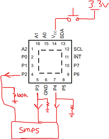
    So how I understand the issue is that the PCA9534A configured P2, P3, P4 as outputs. On each of these IO's there is a 100k PD resistor to GND. When the IO's are allowed to float or are configured as inputs (default state of PCA9534A), EN = LOW. 

    During a power off event where a push-button disconnects the VCC supply, the PCA9534A VCC is disconnected, the IO's measure a voltage between 1.04V and 1.26V, the expected voltage should be 0V according to the 100k PD, but it seems there is leakage coming from the IO's of the PCA9534A. 

    Testing has shown that the lines are not held at 3.3V as intended but held at 1V-1.2V

    Above, you expect that the IO's are to be held at 3.3V? If the PCA9534A enters a power-reset condition by disconnecting the VCC line, then the device will power on with IO's configured to the default state = CMOS inputs. The PCA9534A will drive the IO's high during a power cycle. 

    This is how I understand the circuit: 

    What is the voltage on VCC doing during the disconnection of the power supply? Are we following the power-on reset requirements as shown in the datasheet? 

    Regards,

    Tyler

  • Hello Tyler,

    Thank you for responding. Your understanding of the circuit is accurate. The push button is a little different since it isn't just a button between the rail and 3.3V, but close enough for this. 

    Unfortunately, due to the physical composition of the PCB, there is a SOM chip above the IO Expander, that can't be moved during operation and I don't have access to VCC on the IO Expander during operation. That is really what I have been wanting to probe, and I am waiting on a custom extension for the connector.  Therefore I can't verify the voltage at the Vcc pins during the various stages of the POR as shown in the datasheet and your screenshot of Table 11-1 above.

    I did do some quick math to determine the reset times between reset events and the ramp times, and noticed that the 0.1uF input capacitor for the IO Expander yields an approximately 1ms ramp time, which is at the lower threshold, so I tested with a 1uF capacitor, but that didn't resolve the issue.

    I would imagine the behavior I am seeing might indicate that the voltage during this shutdown event isn't reaching that 0.2V threshold on the ramp down, but I am still working on getting access to appropriate locations on the PCB to test. 

  • Hi Gavin,

    Sounds good, let me know when you get more information on the measurements. 

    If the PCA9534 goes into reset mode due to power off condition via the switch, then the IO's will become high-z and not output a voltage. Then the 100k PD resistor is pulling the IO low to GND. There is either leakage from the IO expander (which there shouldn't be) or there is leakage coming from the EN pins of the LTC3521 device, what pins are being connected on the LTC3521? 

    Regards,

    Tyler

  • Tyler,

    I was able to take some measurements of the VCC net during the shutdown event, and the root cause of the issue seems to be that during the process the line halts at 1.24V or so. This deviates from the required POR behavior.

    Thank you for your support on this issue.

  • Hello Gavin,

    Please let us know if you have additional questions. Thanks!

    Regards,

    Josh