This thread has been locked.

If you have a related question, please click the "Ask a related question" button in the top right corner. The newly created question will be automatically linked to this question.

TCA9509: TCA9509: TCA9509 SDAA/SCLA PIN input leakage current test condition?

Part Number: TCA9509

During testing of the TCA9509, I found that the input leakage current values for SDAA and SCLA do not match the specifications in the datasheet. My test conditions are as follows:
1. EN = VCCA, VCCA = 1.8V, VCCB = 3.3V, SCLB = 3.3V, SCLA = VCCA. Under these conditions, the input leakage current of SCLA is approximately 50 µA.
2.EN = VCCA, VCCA = 1.8V, VCCB = 3.3V, SCLB = 0V, SCLA = 0.2V. Under these conditions, the input leakage current of SCLA is approximately 100 µA or higher.
Furthermore, when EN = 0V, the measured input leakage current of the TCA9509 still does not match the datasheet specifications.
 
Since the TCA9509 datasheet does not provide detailed test conditions for input leakage current, could you please provide the corresponding test conditions and confirm whether the input leakage current test results for the TCA9509 are consistent with the datasheet?

  • Hi Wenjie,

    We are still looking into this and will provide an update shortly.

    Regards,

    Jack

  • Hi Wenjie,

    1. EN = VCCA, VCCA = 1.8V, VCCB = 3.3V, SCLB = 3.3V, SCLA = VCCA. Under these conditions, the input leakage current of SCLA is approximately 50 µA.
    2.EN = VCCA, VCCA = 1.8V, VCCB = 3.3V, SCLB = 0V, SCLA = 0.2V. Under these conditions, the input leakage current of SCLA is approximately 100 µA or higher.
    Furthermore, when EN = 0V, the measured input leakage current of the TCA9509 still does not match the datasheet specifications.

    What does your bench setup look like? 

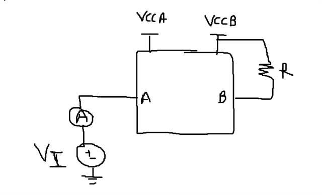
    I think the bench test looks something like this

    Where the input voltage VI corresponds to VCCA or 0.2V, an ammeter is placed in series with the A-side with no pull-up resistor. VCCA and VCCB are powered according to the electrical characteristics. A pull-up connects B-side. 

    Regards,

    Tyler

  • Dear sir:
            Our test method is consistent with the one shown in your diagram.
    1. When testing leakage with SCLA = VCCA, the B port is pulled up so that SCLA outputs a high level. The measured leakage current in this case exceeds the 10 μA specified in the datasheet. We analyzed that this occurs because the A side is pulled up by an internal 1 mA current source. If a voltage of VCCA is applied to SCLA, it actually higher than the source of the internal 1 mA PMOS transistor (due to the parasitic resistance), resulting in reverse current injection—approximately 50 μA.
    1. When testing with SCLA = 0.2 V, the corresponding SCLB input a low level so that SCLA outputs approximately 200 mV. The leakage current measured is around 100 μA, which also exceeds the datasheet specification of 10 μA. In our view, the chip’s VOLA is not exactly 0.2 V. Therefore, under the test condition SCLA = 0.2 V, when the external voltage source clamps SCLA at 0.2 V, the external test supply creates a shunting path, leading to the measured leakage exceeding the specification