This thread has been locked.

If you have a related question, please click the "Ask a related question" button in the top right corner. The newly created question will be automatically linked to this question.

DP83TD510E-EVM: Ethernet to SPE and SPE to Ethernet timing data over the temperature variation

Part Number: DP83TD510E-EVM
Other Parts Discussed in Thread: DP83TD510E

Reference link :  DP83TD510E-EVM Evaluation board | TI.com 

We are using a reference design from Texas Instruments for an Ethernet-to-SPE converter. In this design, a 25 MHz external crystal oscillator (ABM8AIG-25.000MHZ-12-2Z-T3) is used, which has a worst-case temperature stability of ±70 ppm.

This 25 MHz clock is provided as an input to the SPE PHY (DP83TD510ERHBR). The SPE PHY uses its internal PLL to generate a 50 MHz reference clock required for the RMII interface and outputs this clock to the Ethernet PHY (DP83822HRHBT).

Since the system supports bidirectional communication (Ethernet ↔ SPE) over RMII, the 50 MHz clock is critical for timing synchronization between the two PHYs.

The objective is to verify whether this TI reference design will operate reliably over the temperature range of –40 °C to +85 °C, and to evaluate whether temperature-induced variations (such as oscillator stability and PLL behavior) could impact the timing relationship between the two PHY devices.

  • Hi Shreyas, 

    Our part DP83TD510 has been categorized for the operating temperature range of –40°C to +105°C, which meets your requirement. However, you mention that the input clock has a stability of up to 70ppm, which violates the 510 clock requirements of 50ppm. The frequency impact of temperature seems to be 50ppm over the full operational temperature range up to 125°C, so the total ppm mismatch may still be below 50ppm up to 85°C. As long as the input clock is meeting said requirements, the RMII interface should be robust. 

    Best,

    Vivaan

  • Thanks for the clarification.

    We have selected an oscillator with 20 ppm frequency stability over the full temperature range, so the input clock requirement is satisfied.

    In your previous response, you mentioned:

    “As long as the input clock is meeting said requirements, the RMII interface should be robust.”

    We would like to confirm the meaning of “RMII interface robust” in our application.

    Specifically, does this mean that the RMII communication link between:

    1. Ethernet PHY (DP83822HRHBT) → SPE PHY (DP83TD510ERHBR), and

    2. SPE PHY (DP83TD510ERHBR) → Ethernet PHY (DP83822HRHBT)

    will remain reliable and stable across the entire operating temperature range of –40°C to +85°C, provided the input clock meets the required specifications?

    Please confirm whether the RMII data communication between these two PHY devices is guaranteed to remain robust over the full temperature range under these conditions.

  • Shreyas,

    As long as the timing requirements for the input clock and the RMII signals is met, the RMII interface should be robust. The clock you selected seems to have 20ppm variance throughout the full temp range, so I expect that should not cause any problems. The setup and hold time variations may still cause some issues depending on your application, but those parameters can be tweaked as needed.

    Best,

    Vivaan

  • How can the setup and hold time be Tweaked as needed—through software configuration or by hardware provisions? Could you please explain in very detailed terms how setup and hold time variations can be tuned or modified?

    Please also specify the maximum junction temperature (Tj max) for the DP83TD510ERHBR Single Pair Ethernet PHY IC. According to the TI DP83TD510E datasheet, the device is rated for an operating ambient temperature range of –40°C to +105°C

  • Shreyas, 

    Setup and hold times can be tweaked both through software configuration and hardware provisions using longer traces. On the 510, register 0x0017 bit 8 can be used to induce a delay if the PHY is set to RMII Master. You can use either method depending on your specific application.

    The junction temperature depends on the power dissipation under your application, but we do not expect it to go over 125°C.

    Besst,

    Vivaan

  • We have completed EFT immunity testing on the EUT and monitored Ethernet-to-SPE communication performance during the test.

    Observed Results:

    • 500 V EFT: Communication stable with 0% packet loss
    • 1 kV EFT: Communication active, but 4–5% packet loss observed
    • 2 kV EFT: Communication failure

    Current Status:
    The design performs acceptably at lower EFT levels, but fails to meet robustness requirements at 2 kV. To ensure compliance and achieve stable communication with minimal or zero packet loss across all required EFT levels, especially at 2 kV, further hardware optimization is necessary.

    Target Objective:
    Achieve:

    • 0% packet loss at 500 V
    • 0% packet loss at 1 kV
    • 0% packet and Stable communication without failure at 2 kV

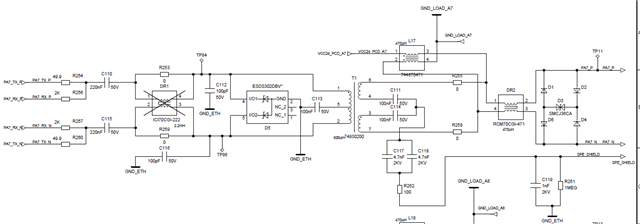
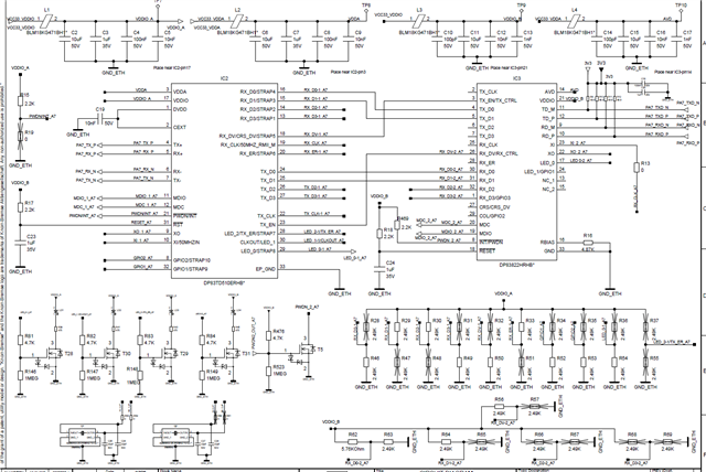
    Please review the schematic and suggest required hardware modifications, layout updates, and protection enhancements to improve system immunity and ensure compliance with EFT requirements.


    1st Schematic: Ethernet to SPE communication using 2 Phys.

    2nd Schematic: CDN Network (Coupling Decoupling Networking)

    Flow is from Ethernet Phy to SPE Phy then through CDN Network and then next to relay

  • Shreyas, 

    There are a few points that may help in getting better EFT immunity test results. I assume you are referring to the IEC 61000 4-4 EFT test, in which the high frequency pulses are sent to the ethernet cable through capacitive clamping. 

    One of the biggest gaps in this test is using shielded cables, are you using shielded cables for these tests? The high frequency bursts can usually find a path through the shield to the connector ground, which should help in EFT immunity.

    If shielded cable are used for EFT testing, the main concern is the low impedance path between the connector ground to earth ground. Similar to ESD testing, a good ground path can reduce the potential ground bounce and reduce the common mode voltage injected into the system.

    It seems like there is no ground isolation being used. This is highly recommended for better performance to reduce ground bounce in the system. Additionally, a ground layer below the MDI lines in the layout can help in better impedance matching, if not already present.

    This Application Note also covers this test and some details about the setup. It seems like this result is matching your requirement. The reference design board used for these tests is the TIDA-010261, which can be found here for schematic/layout reference.

    Best,

    Vivaan