This thread has been locked.

If you have a related question, please click the "Ask a related question" button in the top right corner. The newly created question will be automatically linked to this question.

SN65LVDS93A: Regarding the LVDS data output from the SN65LVDS93A

Part Number: SN65LVDS93A

HI TEAMS

We are currently planning to use the SN65LVDS93A to drive the LCD panel. As shown in the figure below, purple represents /SHTDN (pin 26), and blue represents the LVDS data. I would like to know what data appears between the moment when /SHTDN (pin 26) is driven high and the moment when the data becomes valid (the area marked in the red box below). Is this portion of data software‑controllable? What pattern does it display?When performing the backlight‑enable control, should the data within the red‑boxed area in the figure be taken into consideration? Or can it be regarded as invalid data that does not need to be considered? 

 Thank you.
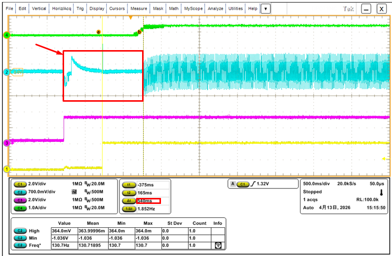
image.png

Green: BKLT_CURRENT, Blue: LVDS Data, Purple: LVDS_SHTDN_N, Yellow: VCC (3.3V)

  • Hi Boris,

    I would like to know what data appears between the moment when /SHTDN (pin 26) is driven high and the moment when the data becomes valid

    This will depend on what video is being sent from the video source. Below is a screenshot of the power up sequence requirements:

    Power up sequence for SN65LVDS93A

    Based on this, the video source should start sending video data (black screen) before the SHTDN signal is brought high. After a 1ms wait (post SHTDN toggle), the chip should be phased locked and will display the black video. It is only after this that the video source should transition to the desired video data and the backlight for the panel should be turned on.

    Is this portion of data software‑controllable?

    Not in terms of the LVDS93A, this will be controlled by the video source.

    What pattern does it display?When performing the backlight‑enable control, should the data within the red‑boxed area in the figure be taken into consideration? Or can it be regarded as invalid data that does not need to be considered? 

    If the power up sequence from the datasheet is followed, it should produce a black screen before the backlight is turned on. After the backlight is turned on, the video source will have already switched to active video and the black screen is never seen.

    If the power sequence is followed as it is shown in the datasheet, the red highlighted portion of data does not need to be considered.

    Best,

    Cameron

  • HI Cameron 

    Thank you for your reply. It was very helpful. However, I still have a few questions that I would like to confirm with you.

    ①Regarding item 4, “Toggle LVDS83B shutdown to /SHTDN = VIH,” does “LVDS83B” refer to the SN65LVDS93A, or does it refer to a specific register?

    ②For the red‑boxed portion in the figure, can I consider it as invalid data sent by the SoC? Or, according to the correct power‑up sequence, should this portion actually be black‑screen data, and the data after the red box is the valid data? Is my understanding correct?

    ③My understanding is that the backlight should be enabled only after delaying for a certain period of time following the transmission of valid data. Is that correct?

    Thank you.

  • Hi Boris,

    Regarding item 4, “Toggle LVDS83B shutdown to /SHTDN = VIH,” does “LVDS83B” refer to the SN65LVDS93A, or does it refer to a specific register?

    That refers to the SN65LVDS93A. The LVDS93A is a spin of the LVDS83B chip, so it shares much of the same datasheet technical information, which is why the LVDS83B is referred to there.

    For the red‑boxed portion in the figure, can I consider it as invalid data sent by the SoC? Or, according to the correct power‑up sequence, should this portion actually be black‑screen data, and the data after the red box is the valid data? Is my understanding correct?

    The second part is correct here. Ideally, the SoC will send black data during that portion of the power on sequence, and then the back light will be turned on after the wait period and after the SoC has switched to normal video. 

    My understanding is that the backlight should be enabled only after delaying for a certain period of time following the transmission of valid data. Is that correct?

    The more important delay is the one where the SoC is sending black data, since this will allow the device to become phase locked to the video. After that, there will inherently be some small delay between switching to valid/regular video and when the backlight is turned on, but that will be dictated by your SW configuration for your SoC. 

    Best,

    Cameron