Part Number: SN74LXC8T245
Hi Ti Forum,
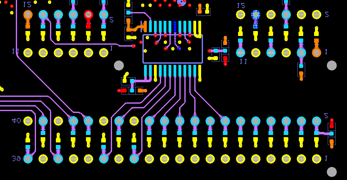
I would like to know if adding TVS diodes to the B side of the device is necessary for improved circuit protection beyond what the IC provides or handles. I have a complex pcb with 14 voltage level translators set as either input or output. The B side signal paths are routed to THMT headers that provide the off board path. Currently every signal pin has an added TVS diode within 1mm of the pad. Our contract assembly house needs more space between the TVS diode and pad for selective soldering process. The spacing needed is 5mm and placing the TVS diode this far from the pin reduces effective protection. The pcb board is dense and I am inquiring if the TVS diodes are even needed especially when the SN74LXC8T245PWR has listed ESD protection that exceeds JESD 22 – 4000-V Human-Body Model – 1000-V Charged-Device Model . The TVS diode will most definitely provide more protection, however, it is indeterminate at this time whether the internal IC ESD protection,which is not listed in the documentation, or the TVS diode will conduct and protect first.
What are IEC 61000-4-x specifications for this IC?
What is the IC's ESD internal protection architecture?
The TVS diode provides for ESD +-10/15KV (IEC 61000-4-2) , EFT 40A 5/50ns (IEC 61000-4-4 ), and Lightning 5A 8/20us (n, IEC 61000-4-5).
I would like to know your opinions and insights to determine if the TVS diodes are even necessary.
Board space is limited on both sides and I can possibly shift many headers and TVS diodes and create an ESD Protection Zone between the headers and the voltage level translators. I need to address all issues, evaluate all options, and fully test before full production begins over+25K boards.
What are the advantage and disadvantages?
A picture of the TVS diode placement is provided below.
Sincerely,
David