This thread has been locked.

If you have a related question, please click the "Ask a related question" button in the top right corner. The newly created question will be automatically linked to this question.

THVD2450V: Unexpected low output at R pin when IEC61000-4-4

Part Number: THVD2450V

Hi team,

Customer test IEC61000-4-4 (Fast Transient) test on the communication line.

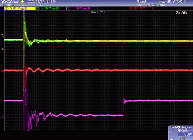
CUstomer see R pin is toggled to Low from High for 11us even no communication is taken. Actually there were noise on the differential signals, but the "11us low output" seems not match to the actual noise pulse width.

Additionlay, customer tested it with having A and B shorted, but R pin doesn't go Low.

What is considered as the reason of R pin being toggled to Low? In what timing R pin become Low output?

Regards,

Hayashi

  • Hi Hayashi,

    First, no transceiver guarantees the communication output during ESD testing such as IEC 61000-4-4 (EFT). However, we do guarantee that our transceiver will survive without damage under the conditions listed in the datasheet. 

    Second, this 11us time they are seeing on the output is expected, and a feature of this device is being triggered by the EFT. The reason they see a ~11us glitch is due to the fail-safe timer built into this device. Please reference time tD(OFS) and section 7.3.5 in the datasheet. Essentially there is a ~10us delay where R is held low, then after that point R is active high. 

    Best,

    Ethan

  • Hi Ethan,

    Thank you for clarifying that the operation is not guaranteed during ESD testing. That's fine.
    However, I would like to ask — when the initial logic state is High, is the behavior where the output first goes Low and then returns to High after a certain period (=tD(OFS)) also considered an expected behavior? From my reading of the datasheet, it appears that only the transition from Low to High is described, and I was not able to find a description covering this High → Low → High transition.
    Best regards,
    Hayashi
  • Hi Hayashi,

    Could you share waveforms of exactly what they are seeing? Any chance they have the enable pins shorted (DE and /RE)? Do they short the bus cables together during the test or is only one pin tested (either A or B)?

    You are correct; there is no description in the datasheet of the high-low-high transition. But it all comes down to the exact VOD voltage. Below is an example where the R output is high-low-high:

    Although that screenshot is a very different scenario, it shows that it is possible in edge cases (green line is the R pin). The VOD has to be within the VTH_FSH threshold for it to trigger in this case. The bottom line is that when the R pin is driving low for ~10us, the transceiver is showing that the VOD is crossing into the "undefined" threshold of about -40 to 40mV during the transient.

    Best,

    Ethan

  • Hi Ethan,

    I attach the waveform. RE=GND, DE=Pull-down, VIO=VCC=5V.

    Yellow and Green: A and B (Not connected to host)

    Red: Differnetial signal (A-B)

    Purple: R pin

    Regards,

    Hayashi

  • Hi Hayashi,

    That behavior is expected. There is enough differential noise on the A-B pins such that it triggers the failsafe timer. 

    If anything, the R pin toggling low should help the customer identity that there was a transient condition present. This could help indicate to the MCU that there could be a communication failure. 

    Additionlay, customer tested it with having A and B shorted, but R pin doesn't go Low.

    Because these pins are shorted together there is no A-B differential voltage that triggers the failsafe timer. 

    Best,

    Ethan