This thread has been locked.

If you have a related question, please click the "Ask a related question" button in the top right corner. The newly created question will be automatically linked to this question.

DS25CP152: Input hysteresis and output LVDS swing

Part Number: DS25CP152
Other Parts Discussed in Thread: SN65LVP19

Dear support,


I'm working on a special hardware architecture to clock a aquisition system.
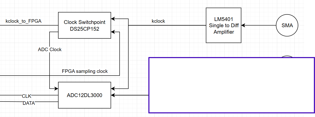


image.png


Righthand top you find a analog 50Ohm input. A clock single ended input with a frequency range of 400MHz ... 1,1GHz. I will use LM5401 to convert it to differential signal and let the ADC digitize it.

As a parallel hardware path, I want to use this differential output of LM5401 to drive DS25CP152's second intput. Here are my first questions: Is there any hysteresis in DS25CP152 or is that reflected in the propagation delay of 500ps? It this propagation delay dependent on the rise-time of the clock? Is the propagation delay constant over liefetime and temperature, e.g. can I parameterize it and use a phase-correction algorithm in SW?

I will decouple the signal between LM5401 and DS25CP152 with capacitors and rebias it tho DS25CP152's common mode input. Any comment to that?

The LVDS output of DS25CP152 is specified as 250mV to 450mV differential. ADC12DL specifies minimum input swing of 0,4V. In the following picuter of DS25CP152's datasheet I wonder if DS25CP152  has rather 500mV to 900mV swing.
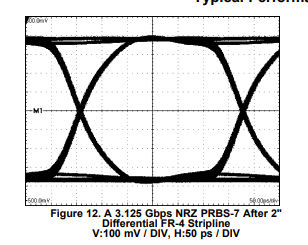
image.png


Kind regards,


Simon

  • Hi Simon, 

    We don't have any hysteresis spec'd for this device, but the propagation delay should have that factored in. It measures the time it takes the VOD to cross 0V from when the VID crosses 0V (Figure 6). Regardless, if you are wanting to know how the propagation delay will change for a given device across its recommended operating conditions, you can use the random jitter spec (t_RJ) for clock signals. For example, if you give a 1.1 GHz clock signal as an input, the output will only deviate 0.5ps from its expected edge.

    For re-biasing the ac-coupled LVDS signals, you can refer to this app note for some examples on how to do that: https://www.ti.com/lit/ab/slaa840/slaa840.pdf?ts=1777475402421&ref_url=https%253A%252F%252Fwww.google.com%252F 

    For your question on Figure 12, that is showing the differential output voltage swinging between +400mV and -400mV which is within spec limits. The center horizontal line with the "M1" label is 0V. 

    Regards,

    Matt

  • Hi Matt,

    Thanks or the App-Note. Very interesting read.

    For your question on Figure 12, that is showing the differential output voltage swinging between +400mV and -400mV which is within spec limits.

    -400mV up to 400mV is in my opinion 800mV differential swing. That would be good, ADC12DL needs more then LVDS spec. I cannot link the  DS25CP152 table spec of 250mV to 450mV against the picture figure 12. It seems "doubled" to me. Please clearify.

    Kind regards,

    Simon

  • Hi Simon, 

    That is incorrect. The differential output voltage is the voltage difference between OUT+ and OUT- pins. For example, if the single ended voltage (measured with respect to GND) of the OUT+ pin is 1.4V and the OUT- pin is 1.0V, the differential voltage between those 2 pins is 400mV. If the logic state is inverted and OUT+ becomes 1.0V and OUT- becomes 1.4V, the differential voltage will be -400mV. In the datasheet, the VOD spec limit is described as an absolute value (sometimes written as |VOD|), meaning that it represents positive and negative values. For example, if the typical VOD spec is 350mV, this means the voltage between OUT+ and OUT- will be +350mV for a logic HIGH state and -350mV for a logic LOW state.

    What you described as the "differential swing" was assuming OUT+ has a single ended voltage of 400mV and OUT- at -400mV, which is not what this device does. 

    Figure 12 is not showing the raw LVDS signals. It is using a Math function on the oscilloscope to calculate the differential voltage by calculating the voltage difference between 2 channels where one channel is on OUT+ and the other is on OUT-. Hence the "M1" label on the curve. 

    The TIA-644 LVDS standard state that and LVDS steady state output voltage should be between 247mV and 454mV. If that ADC needs more than that, and LVDS device won't work since that technically isn't an LVDS signal anymore. You might be needing LVPECL instead. If that's the case, something like SN65LVP19 could work. 

    Regards,

    Matt