This thread has been locked.

If you have a related question, please click the "Ask a related question" button in the top right corner. The newly created question will be automatically linked to this question.

TCAN1051H-Q1: TCAN1051H-Q1 and TXS0108E ICs Failure

Part Number: TCAN1051H-Q1
Other Parts Discussed in Thread: LM5013, LM5013-Q1, WEBENCH-CIRCUIT-DESIGNER

Hello there,

TCAN1051H-Q1 
TXS0108EQPWRQ1 

Issue: The CAN ICs are blown, and the TXS0108 IC is also non‑functional. 

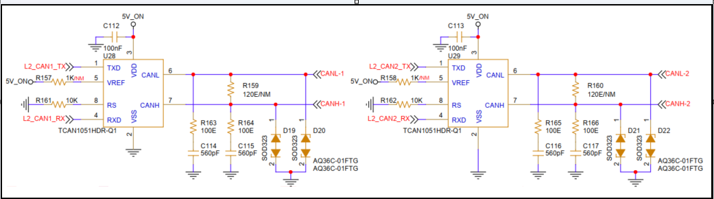
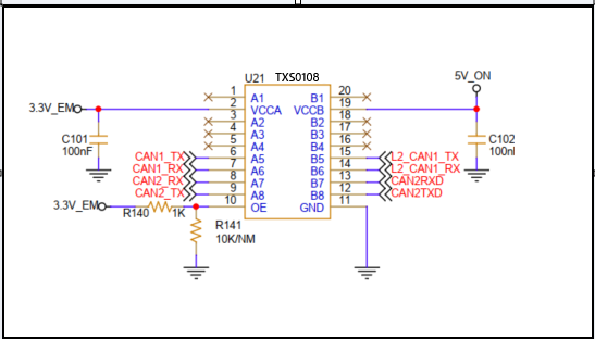
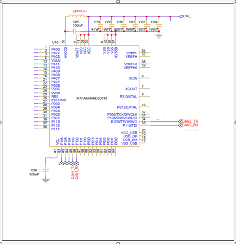
We are using the TXS0108EQPWRQ1 in our product for the CAN Transceiver–Microcontroller communication line, where it functions as a level shifter from 5V to 3.3V. In our design, Port A is connected to 3.3V and Port B is connected to 5V.

We checked both CAN ICs and TXS0108;  there is no short circuit between VCC and GND, nor pin‑to‑pin. 
We can barely see that both CAN ICs have been blown; the area of the IC that is blown is between the VCC and GND pins. (Pin no: 2-GND and 3-VCC)

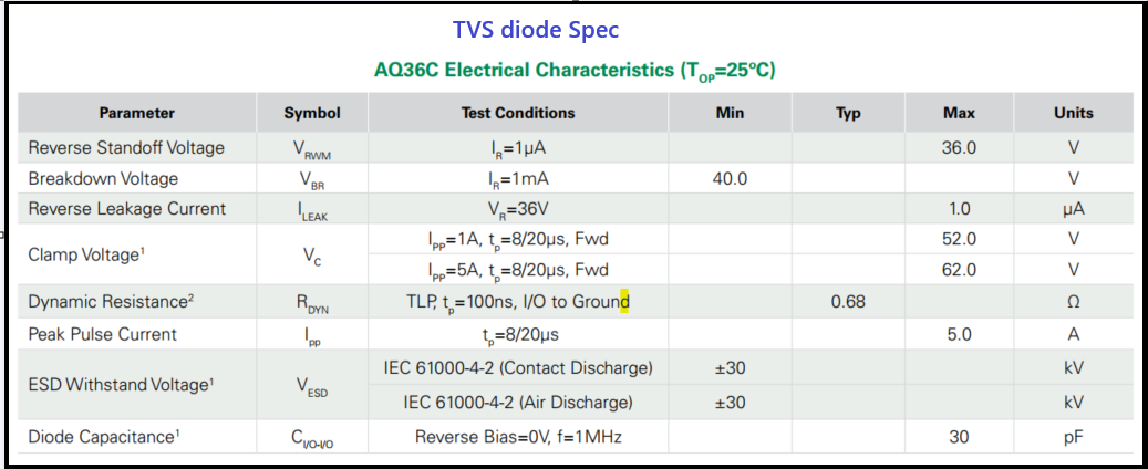
We checked the TVS diode (AQ36C-01FTG) resistance, which shows OL, indicating it is good.
We then replaced the CAN ICs and tested, but no data was received.
After replacing the TXS0108 IC, the device started working.                                                                    We will share the schematic and images for your reference. 

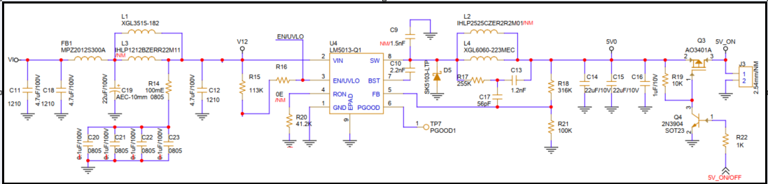
Additionally, we are using the (TI) LM5013‑Q1 IC in the design for 5V out, and I will provide the LM5013‑Q1 circuit schematic as well. 
Both the CAN IC and TXS0108 IC share the same 5V_ON supply. 
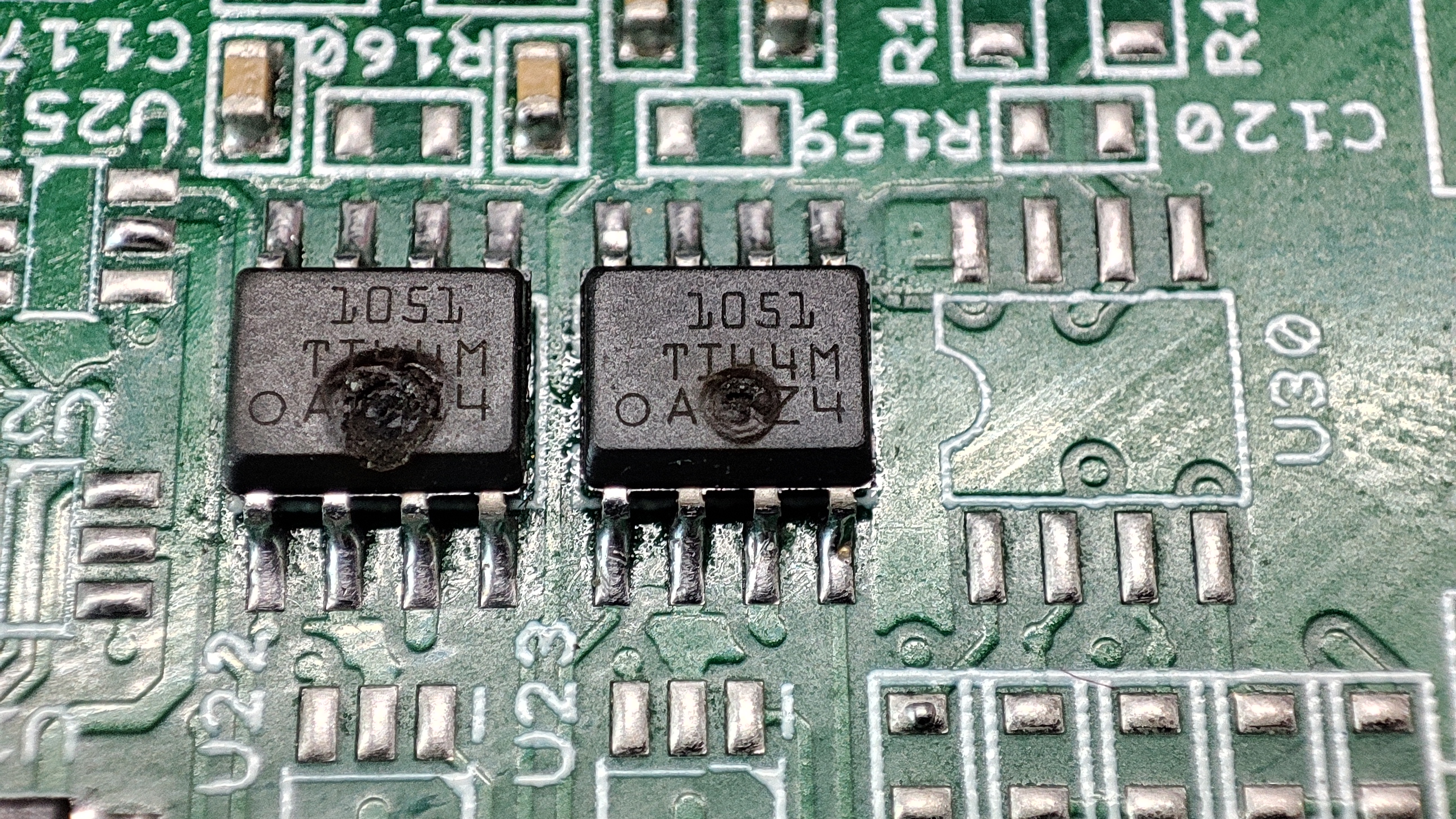

CAN ICs.jpg

image.png

image.png


image.png

image.png

Please advise on:

  1. The possible reasons for this failure

  2. Recommended checks or diagnostic steps to identify the root cause

Your support in resolving this issue will be greatly appreciated.

  • Hi Narendraprasath,

    Please note that you seem to be using a bidirectional level shifter and the TCAN schematic further shows both TXD and RXD going into the device.

    However, RXD should be an output going out. Hence, damages may imply the device most likely experienced higher than the abs max ratings.

    Furthermore, 560 pF seems too large for proper communication as we recommend 100 pF max for slower data rates and would further recommend removing the 560 pF + 100E on CANH/CANL to double confirm while completely isolating all other nodes to help narrow down as needed. I also presume VREF is actually the NC-option used. If not, recommend including a decoupling cap on each power supply pin similar to figure 11-1 of the data sheet, thanks.

    Best Regards,

    Michael.

  • Hello Michael,


    Hope you're doing well, 

    Could you please clarify the first point, which you mentioned in your reply?

    (Please note that you seem to be using a bidirectional level shifter, and the TCAN schematic further shows both TXD and RXD going into the device.

    However, RXD should be an output going out. Hence, damages may imply the device most likely experienced higher than the abs max ratings)

    We would like to clarify certain points for better understanding:

    The TXD is connected to the MCU RX pin, and the RXD is connected to the MCU TX pin. Please refer to the schematic attached below for your reference.


    Regarding the 560pF capacitor, in our device, we are using 250 Kbps speed on both channels. If we change to 100pF, will proper communication be achieved?
    Additionally, what would happen if we use 500 Kbps speed with 100pF?

    The VREF pin is actually NC. We are not adding the R158 and R157 resistors to the IC.

    As you mentioned, the device most likely experienced conditions exceeding the absolute maximum ratings. Could you please specify which pins experienced values higher than the absolute maximum ratings?

    Finally, please explain the reason, how, and why this issue occurred, and provide us with a solution to prevent it in the future.

    Thank you for your support.

  • Hi Narendraprasath,

    My first comment is to clarify the TCAN schematic showing RXD being used as an input. However, this is an output pin for the TCAN device. Also, the TXS device is bidirectional and it shows L2_CAN1_RX is going into the RXD pin of the TCAN device and also into the B6 pin of the TXS device. The corresponding pin of the TXS device (A6) is also shown as an input into the TXS device, connected to CAN1_RX further connecting to the MCU.

    Please clarify as B6 and A6 are shown as both inputs. I.e., 1 should be an input and the other an output. Hence, the RXD pin of the TCAN device should be an output going into an input of the TXS device (B6 for example) and out of A6 into P103 of the MCU / directly going into the MCU if the case. 

    Hence, if the directions are misaligned and the TCAN's RXD output pin is being used as an input, then I suspect some bus contention. If so damages may be expected if and any chance such contention causes the IC pins to observe > than the rated abs max ratings.

    Yes, 100 pF is the max recommended as shown in the switching characteristic section of the data sheet. As speed increases, the bus cap could be reduced, rather than increased. Hence, proper communication can be achieved.

    Furthermore, I can not tell what specific pin as this could be from any of the max rating spec. However, so far I suspect bus contention from the RXD observation as a possible reason and avoiding contention as a solution (by ensuring the output pin is not used as an input), thanks.

    Best Regards,

    Michael.

  • Hi Michael,

    I would like to clarify a few more details regarding the specifications and schematic connections.

    As per the MCU datasheet, Pin 45 is an output (TX), and Pin 46 is an input (RX).

    Please check the screenshot images below for the MCU PINs' Functions and descriptions.


    Regarding the TCAN IC pin functions:

    • TXD is the digital input pin.

    • RXD is the digital output pin.


    The Schematic Connections:

    • TXD pin 1 of the TCAN IC (L2_CAN2_TX) is connected to the TXS input of Port B (B5).
      The TXS output of Port A (A5), CAN1_TX, is connected to MCU Pin 45. MCU Pin 45 is an output (Transmit Data pin).

    • RXD pin 4 of the TCAN IC (L2_CAN1_RX) is connected to the TXS input of Port B (B6).
      The TXS output of Port A (A6), CAN1_RX, is connected to MCU Pin 46. MCU Pin 46 is an input (Receive Data pin).
      It's shown in the image above (MCU Datasheet table).


    These connections are correct, and we have produced over 1000 devices with the same circuit, all functioning properly.

    Issue: One device received from the field reported that data was not being transmitted. At the time of inspection, we found that the TCAN IC had blown.

    Could you please advise on the possible cause and recommend a solution to prevent this issue in the future?

    Thank you for your support.


  • Hi Narendraprasath,

    • "TXD pin 1 (input) of the TCAN IC (L2_CAN2_TX) is connected to the TXS input of Port B (B5)": Two inputs connected and expecting to receive, who is sending? Typo? Should it say TXS "output B5"?
    • "The TXS output of Port A (A5), CAN1_TX, is connected to MCU Pin 45. MCU Pin 45 is an output (Transmit Data pin)": Two outputs connected, who is sending? Typo? Should it say TXS "input A5"?
    • "RXD pin 4 of the TCAN IC (L2_CAN1_RX) is connected to the TXS input of Port B (B6)": This is as expected. RXD is outputting into TXS.
    • "The TXS output of Port A (A6), CAN1_RX, is connected to MCU Pin 46. MCU Pin 46 is an input (Receive Data pin). It's shown in the image above (MCU Datasheet table)": This is expected, TXS outputting into an input.

    If a device is blown, it is most likely due to exceeding the abs max ratings. However, you may actually have to evaluate your system environment to help understand how the abs max ratings could have been exceeded based on your system environment. When narrowed down, then a solution can be recommended.

    Also note that TXS pins can be used as both inputs and outputs. Hence, any chance for bus contention for a case where the TCAN pin contends with the TXS pin with that one device from the field? Or even multiple devices but only 1 stressed significant enough to "be blown"? In essense:

    • Confirm if B5 is always outputting / sending (never inputs / receives) and A5 is always inputting / receiving (never outputs / sends)
    • Confirm if A6 is always outputting / sending (never inputs / receives) and B6 is always inputting / receiving (never outputs / sends), thanks.

    Best Regards,

    Michael.

  • Hi Michel,

    Thanks for your response. I would like to clear points concerning the pin mapping. Sorry for the typo.
    • TXD pin 1 (input) of the TCAN IC (L2_CAN1_TX) is connected to the MCU Pin 45 (output) via TXS level shifter. MCU is the sender here.
    • RXD pin 4 (output) of the TCAN IC (L2_CAN1_RX) is connected to the MCU Pin 46 (input) via TXS level shifter. TCAN is the sender here.
    • As you rightly mentioned TXS device is a bidirectional level shifter so all the pins can support both way of communication.
    We are not suspecting the pin mapping,  MCU and TCAN establishes the proper communication and data exchange happens normally.

    Regarding the point about bus contention, I have checked the MCU software configuration with my team. The specific pins (45 and 46) are configured as CAN bus in the MCU pin configuration at software level, so we can ensure the pins will not act as an other function (like GPIO for example) which will leads to bus contention. So I confirm the following points
    • B5 is always outputting / sending (never inputs / receives) and A5 is always inputting / receiving (never outputs / sends)
    • A6 is always outputting / sending (never inputs / receives) and B6 is always inputting / receiving (never outputs / sends)


    About the failure point. I too agree with your suspect of exceeding the abs max ratings. At the architecture level following part are taken care.
    • We used the bidirectional TVS diode AQ36C-01FTG to protect TCAN IC CAN pin 6 (Low) and 7 (High) and from external transients on the CAN bus, the diode specifications are shared in the first message.
    • We don't see any short circuit or low resistance path in the TVS diodes of the affected device. You can point out if any specific check that we can do.
    • On the power supply side as I mentioned in the first message we are using the LM5013-Q1 stepdown DC-DC converter (5V output) from Texas to power the IC.
    • It's designed as per the Texas's WEBENCH-CIRCUIT-DESIGNER. You can take a look in to the circuit and see if any improvement can be done in the circuit.
    As per my knowledge these are the possible points to exceed the abs max rating which could affect the IC. Kindly suggest if any other circuit area I can look in to?

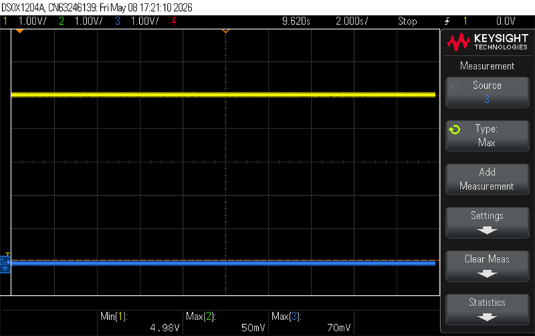
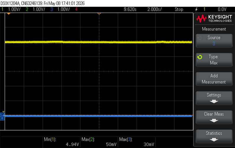
    I'm sharing the voltage waveform of 5V_ON, CANL-1, CANH-1, TXD, RXD by tapping the pins 1, 4, 3, 6, and 7 respectively. The graph is taken with the affected IC. Could you help to understand is there other specific point or any data I can share to narrow down the issue?

    Graph-1
    DSO Graph Details
    Yellow 5V_ON
    Green CANH-1
    Blue CANL-1

    Note: No Inputs are given to the CANH and CANL pins.

    Graph-2

    DSO Graph Details
    Yellow 5V_ON
    Green TXD
    Blue RXD

    Note: No Inputs are given to the TXD and RXD pins. 

    Thank you for your support.

  • Hi Narendraprasath,

    Thanks for clarifying. I would recommend working with your regional TI representative to help submit a customer return for an effective root cause analysis. Please include a known good unit and a failing unit. Hence, we may be able to then evaluate and isolate the failure location to a specific pin(s) area as I believe this should at least provide the clarity needed to further evaluate your system environment, thanks.

    Best Regards,

    Michael.