


Part Number: TSS721A
Hi.
I dont know if it helps, but I feel the need to talk.
I am trying to design a M-Bus slave which is galvanically isolated.
Try1:
This was my first try. As soon as I placed/added R12/R13, to digital isolator IC3 went "active" and draws too much supply current. So the 3V3 supply from VDD (Pin11) breaks down.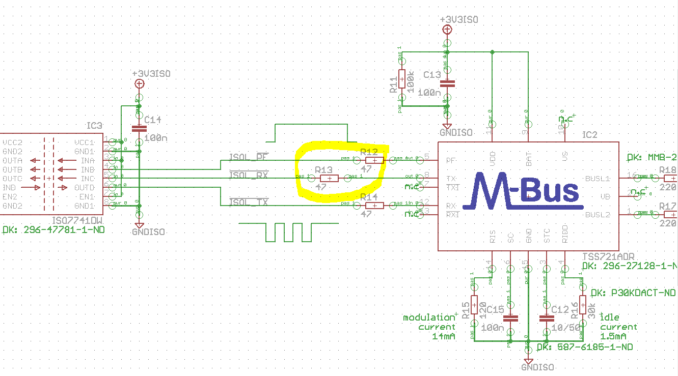
So I went back to the datasheet and did another try, closer to the datasheet example (figure10, basic optocoupler design)
Try2:
I searched an optocoupler with very low diode current. I am using LDA111, which seems to work with less than 1mA of photo diode current.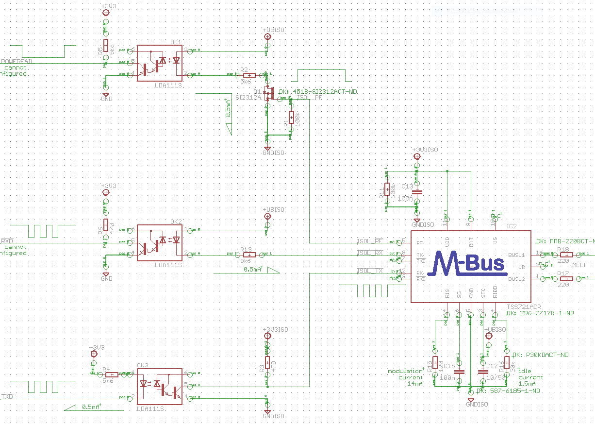
The parts around OK1 and OK2 seems to work properly. Only issue I had, is, that I need to a pretty small R6 as pull up to create kind of rectangular wave form. But at µC side, current is no issue. So my µC is able to receive data from the M-Bus.
But as soon as I added the µC-transmit via M-Bus path (OK3) I have the same issue. R3 must be very small to create proper waveform. But this draws too much current from VDD (Pin11). So the 3V3iso breaks down again.
My problem now is:
1. digital isolators (try1) needing too much supply current.
2. optocouplers either need too much led diode current and/or too much current thru pull up resistor to recover waveform
And with "too much" I am talking about more than 1.5mA, which can be delivered by VDD pin permanently. (In my opinion, the STC pin and the VDD pin can deliver together 1.5mA)
So the datasheet recommends values for different operation modes (e.g. figure 8). But the optocoupler example does not recommend any value at all.
So serious question:
Does somebody ever achived to design an optocoupler application? How to do this with max.1,5mA total usable current?
What optocoupler and values for R4 and R2 are recommended?
Thank you
Matthias


 :
: