This thread has been locked.

If you have a related question, please click the "Ask a related question" button in the top right corner. The newly created question will be automatically linked to this question.

DS26LV32AQML: Application Issues of the DS26LV32AQML

Part Number: DS26LV32AQML
Other Parts Discussed in Thread: AM26LV32,
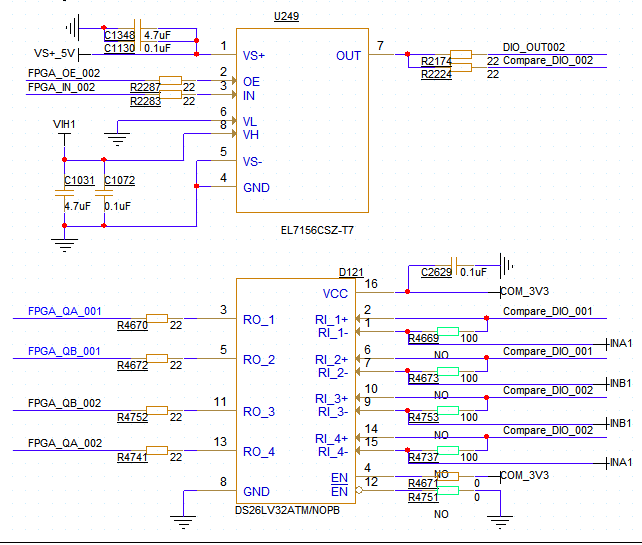
2026-05-11_203455_635.png

In the test circuit ,the el7156 line driver is used to drive signals ,and the DS26LV32 is used as a comparator.when the el7156 is set to tri-state (high-inpedance),the ds26lv32's RI- input is biased at a fixed 2V (INA1=2V  ,INB1=1V , R4669/R4673/R4753/R4737 no-nop).The following behavior is observed on the RI+ PIN :
1. R1+ is floating ,then check RI+ 2V voltage is present .
2. RI+ is pulled down to GND with a 1k resistor ,then check RI+ 2V voltage remains.
3. R1+ is pull down to GND with a 100R resistor ,the voltage drop to near 0V.
why does a voltage appear at the RI+ pin? we look forward to your reply.
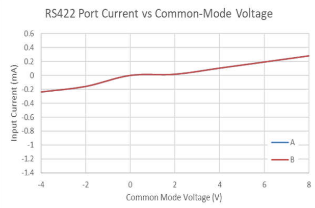
  • The datasheet specifies a typical input resistance of 5 kΩ, and the inputs might have additional pull-up/-down resistors to detect disconnected inputs.

    The AM26LV32 is a similar device with the following typical characteristic (the DS26LV32AQML might behave differently):

  • Hi Yulong,

    There is not much information in this datasheet as it is older, but it does mention that it has receiver open input failsafe. What this means is that it has internal biasing resistors so that the inputs are biased to a particular voltage level. That way when the input pins are left open or floating, the voltage differential isn't in the undefined region. This undefined region is -200mV < VID < 200mV for reference. However, this biasing should be quite weak so that a valid input signal can be driven. This app note describes it well: https://www.ti.com/document-viewer/lit/html/SSZTAK0 

    Best,

    Ethan

  • Thank you for your reply ,’m currently using this chip for the PE electronic pin compare function. I’d like to understand how this floating voltage is generated, why it still has a certain load capacity, and why the measured voltage on pin R+ is 0 when it’s floating.

  • Hi Yulong,

    Here is simplified diagram on the internal receiver input (A pin=RI+, B pin=RI-):


    Additionally, there is some equivalent, differential resistance between the RI+ and RI- pins. Hence, why when you bias one input, the other follows closely. 

    Because RS-422 transceivers are designed for a particular differential communication at a certain common mode voltage. In normal operation, both pins RI+ and RI- are expected to be driven. 

    Best,

    Ethan

  • Thank you for your reply