PCA9557: P0 Protection Diode

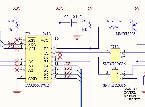
Part Number: PCA9557

In my circuit I detect current flowing into the P0 pin when I connect it to a pullup. There is a diode drop across P0 and VCC.  This is not shown on the diagram.  

image.png

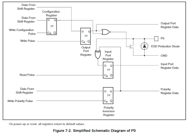
When this part is powered by 3.3V and the P0 input is used as 5V tolerant inputs, is it normal for current to flow into the pin?  If so does this mean the pin can't go higher than VCC + 0.7V and that I must limit the current to 20uA to cmply with the absolute maximum I[IOK] of -20uA.

  • Hello Charles,

    The applications engineer who supports this part is out of office and will return on Thursday. Thank you for your understanding.

    Regards,

    Josh

  • Hi Charles,

    The device supports 5V tolerant I/O's when powered up. This is supported by the VIH spec: 

    Where the VIH spec can be up to 5.5V max regardless of supply voltage. 

    Is there any other device on P0 that is not 5V tolerant? 

    Regards,

    Tyler

  • Here is the circuit:

    • I2C lines - Pulled up to 3.3V
    • SW1 - 3.3V logic
    • U3 - Powered by 3.3V  

    It pulls P0 up to 3.96V, a diode drop over 3.3V.  I replaced the part with NXP's version of the part, and P0 goes to 5V.  With NXP part 500nA flows through R8, R19, Q1's reversed-biased B-C junction.  I don't detect any branch current flowing into P0.  With the TI part, however, it appears like there's a typical 0.7V protection diode from P0 to VCC.  

  • Hi Charles,

    Your logic makes sense here. Based upon the PCA9557 datasheet, I would expect P0 to be pulled up to 5V. 

    I could check this on my own in lab today, but would need to locate a part. Let me get back to you Friday. 

    Regards,

    Tyler

  • I'm interested to hear the results.  As a test I took a TI PCA9557 part of a recently stuffed board and replaced it with a TI part from by parts drawer that I bought years ago.  It behaved the same way.  So I don't think it's just that the contract manufacturer got a reel of defective or counterfeit parts.  

  • Hi Charles,

    I took at look at this in lab. VCC = 3.3V, /RESET = 3.3V, apply a 5V input signal through a 2.2k pull-up resistor on P0. I do not see a diode drop. 

    Do you have an image of the top-side marking of the device? 

    Regards,

    Tyler

  • The parts our CM stuffed were "ATNQ".  The parts from my bin in the lab were "AH8V".  I'm finding they tolerate 5V on P0 when they are powered in their default configuration.  When software configures P0 to an output, however, P0 goes to 0 when configured LOW and roughly a diode drop over VCC.  This suggests it is not simply a protection diode.

    Here are the photographs of the parts.


  • Hi Charles,

    When I plug in the lot trace code from the top side marking, I cannot find the top image 85KATNQ in our system. 

    When I plug in the 54KAH8V code, I find that it traces the PCA9557 device back to one of our fabs. 

    Is it possible to do a diode measurement test on P0 between VCC and GND between the two devices? 

    Regards,

    Tyler

  • My fluke does not see a diode between P0 and VCC on the board or on the unstuffed parts from my bin in the lab.  It sees around 600 kohms.  

  • I've found if I configure the pin as an input, no current flows into the pin.  If I configured it as an output high, some current flows in.  So a successful workaround is to configure it as an input when I want a logic high.  

  • Hi Charles,

    So in summary, the P0-P7 I/O structure seems to be incorrect. It looks like there is some diode structure facing from the pad to VCC when the pin is configured as an input. 

    The feature in page 1 of the datasheet should say 5V tolerant inputs. Not 5V tolerant Input/output. 

    Regards,

    Tyler